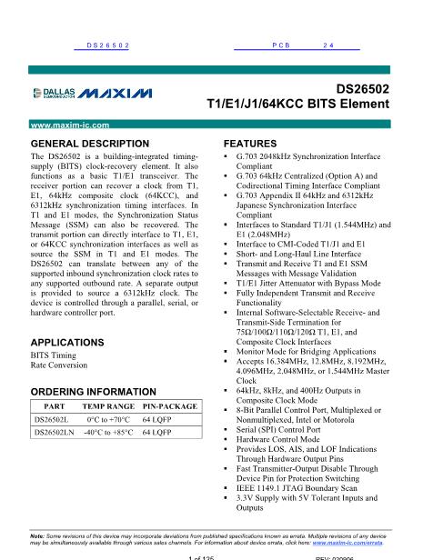
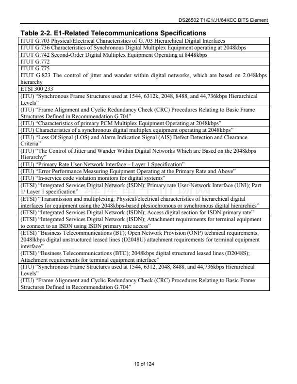
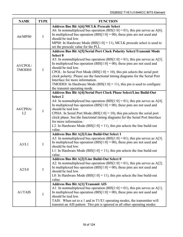
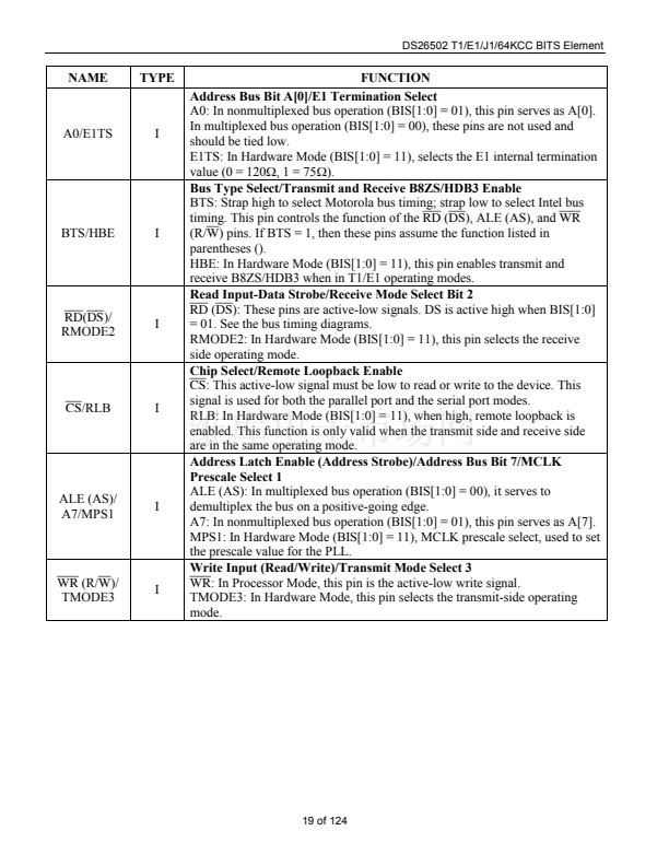
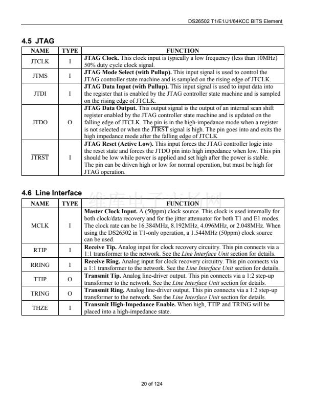
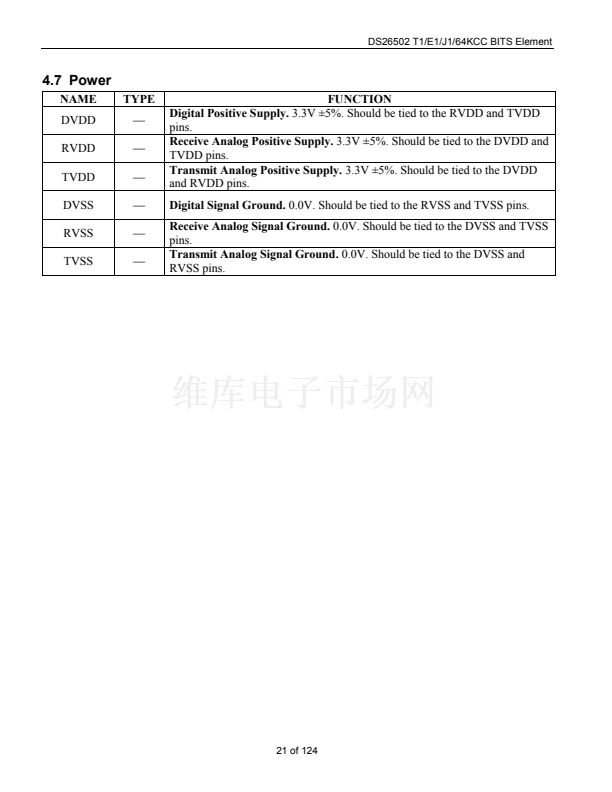
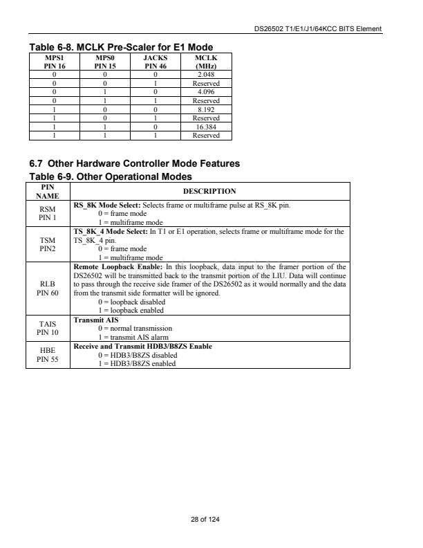
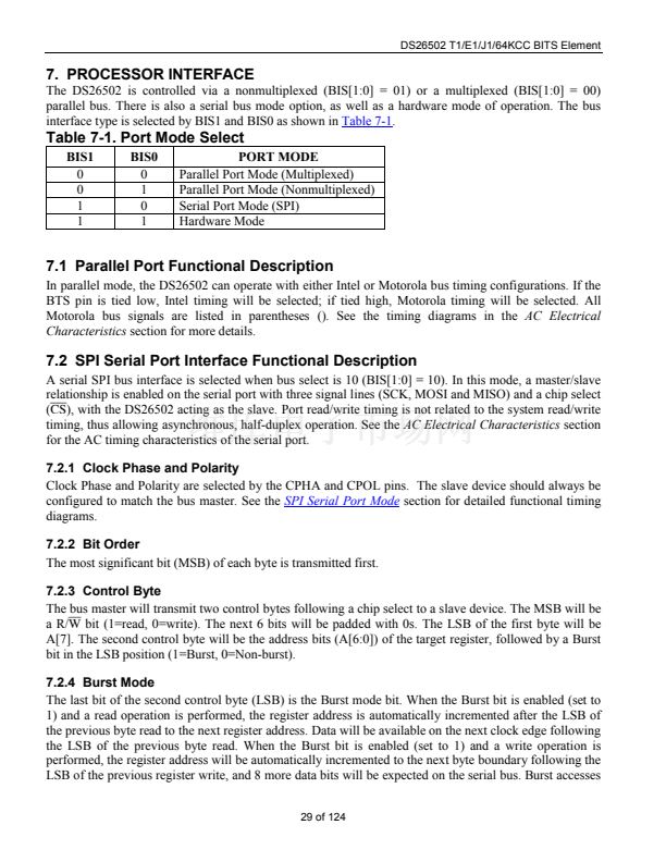
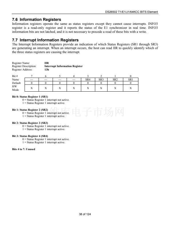
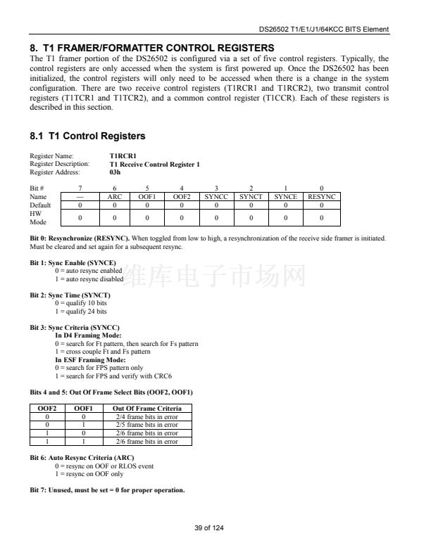
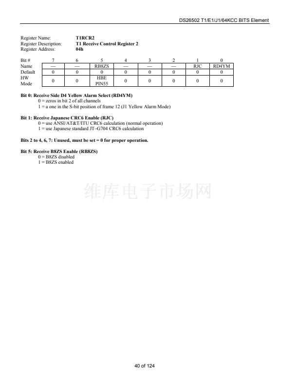
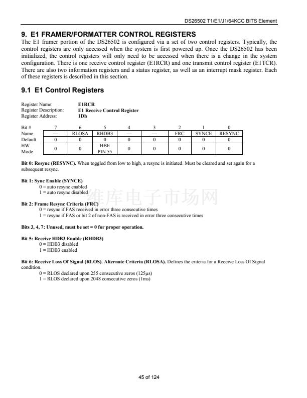
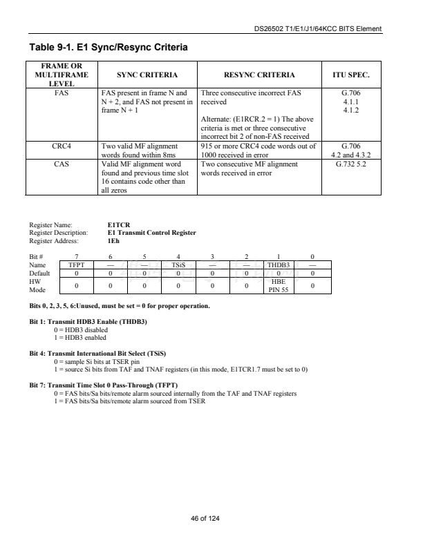
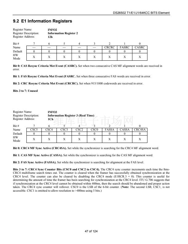
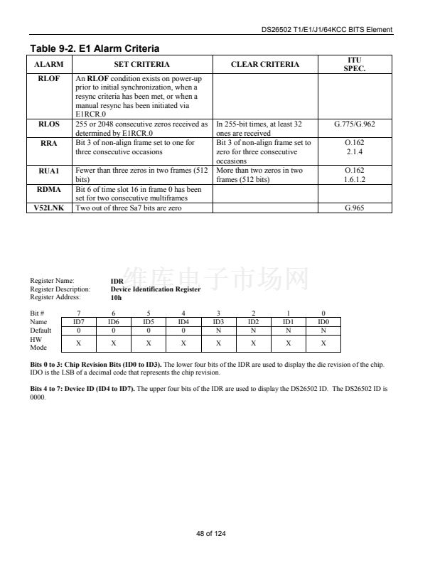
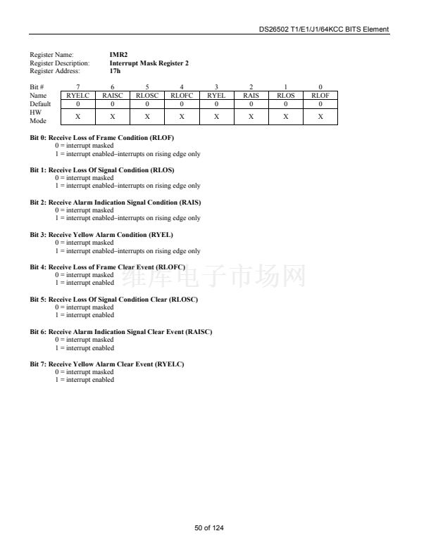
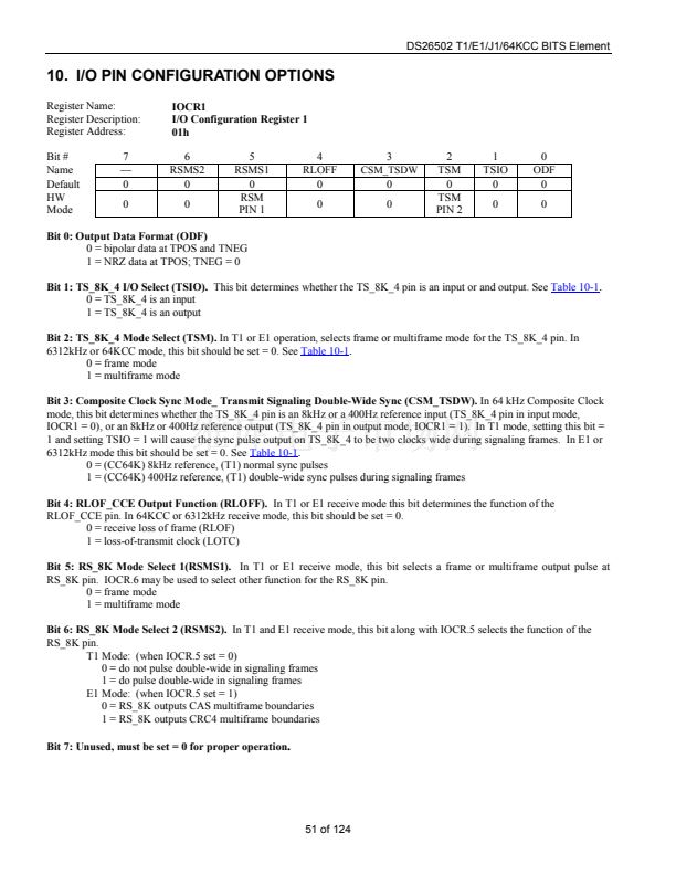
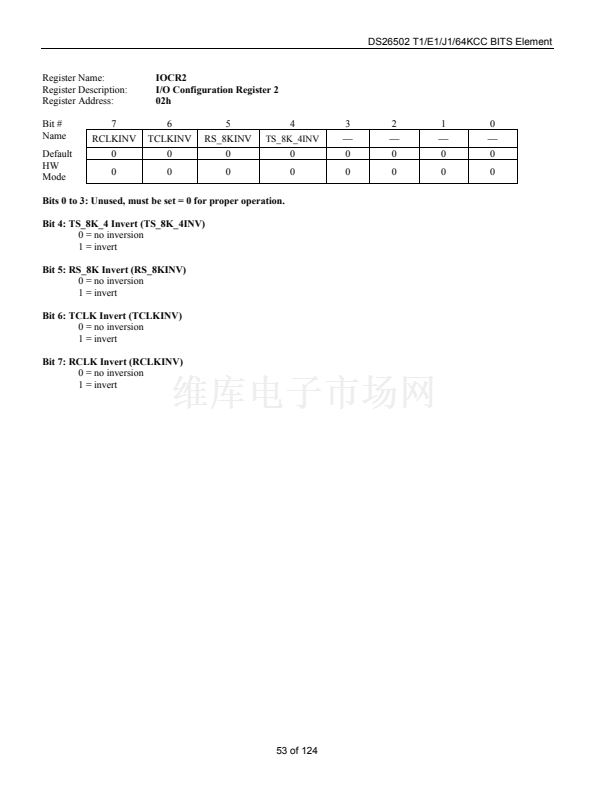
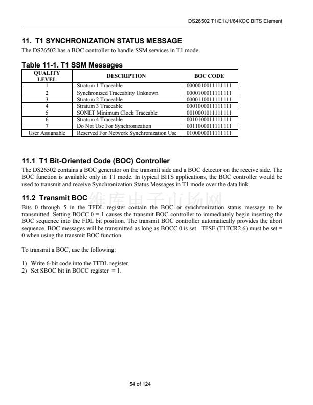
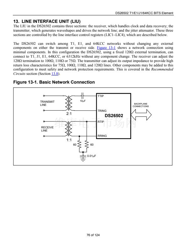
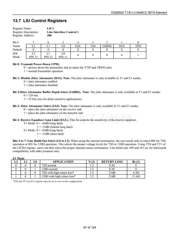
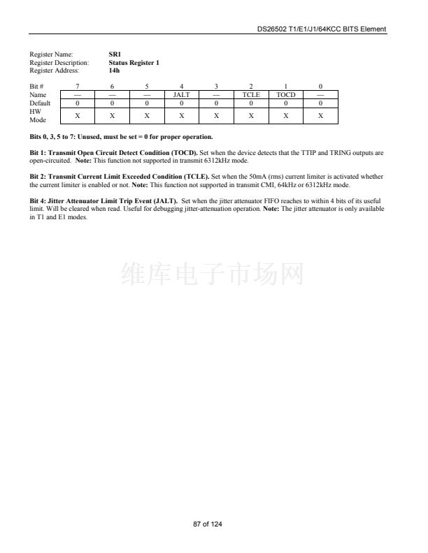
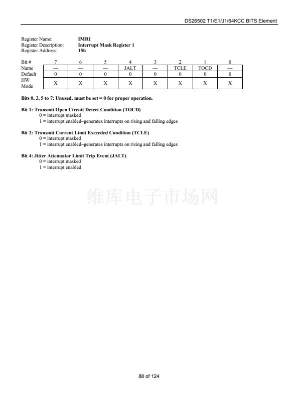
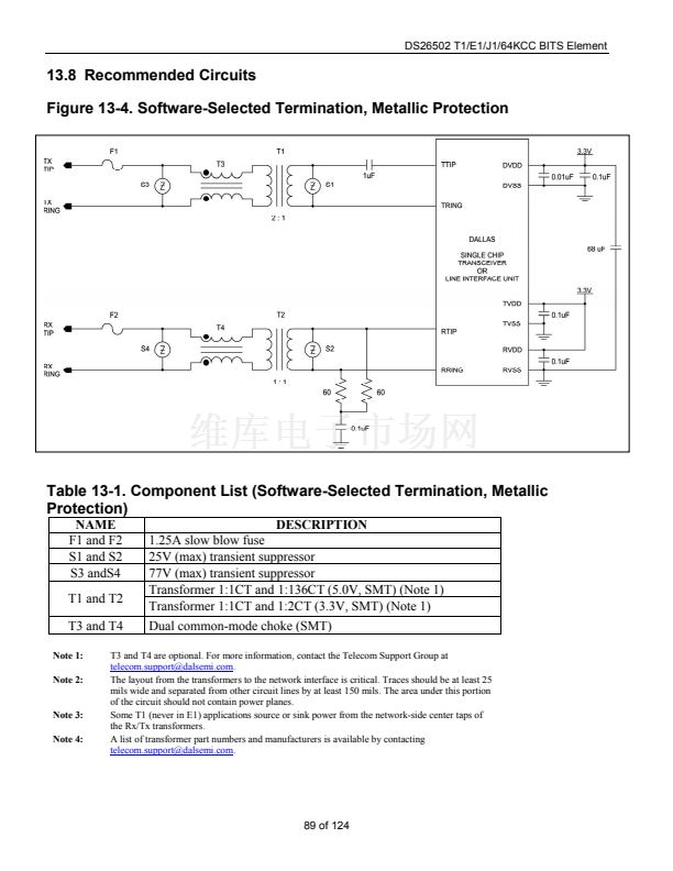
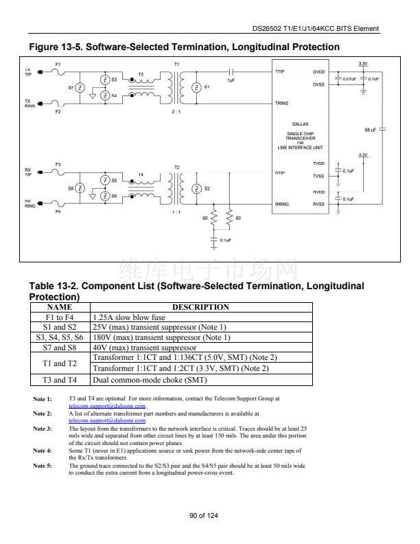
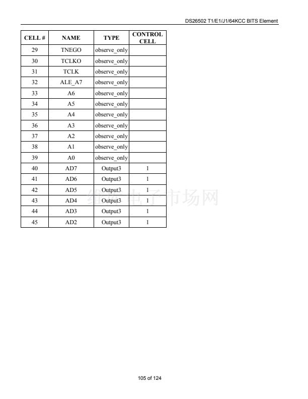
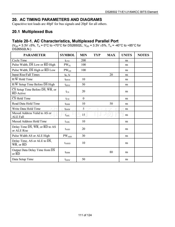
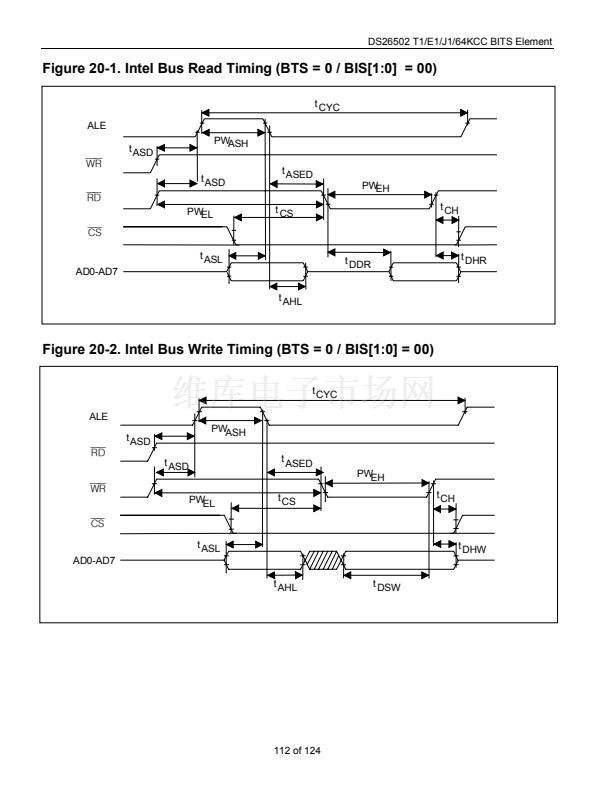
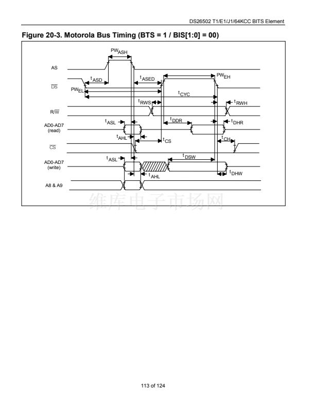
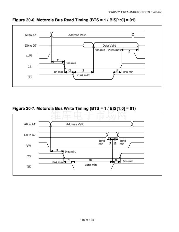
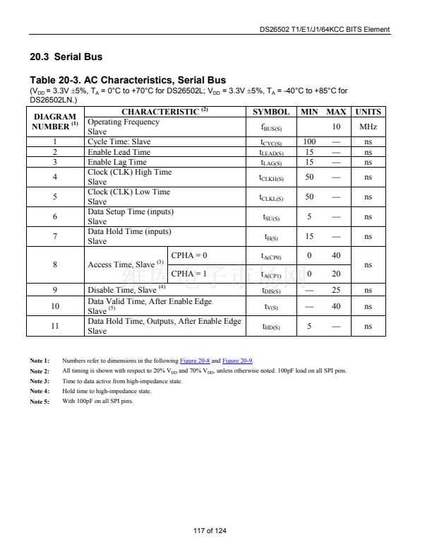
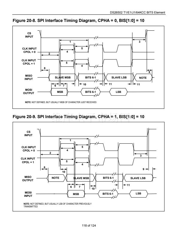
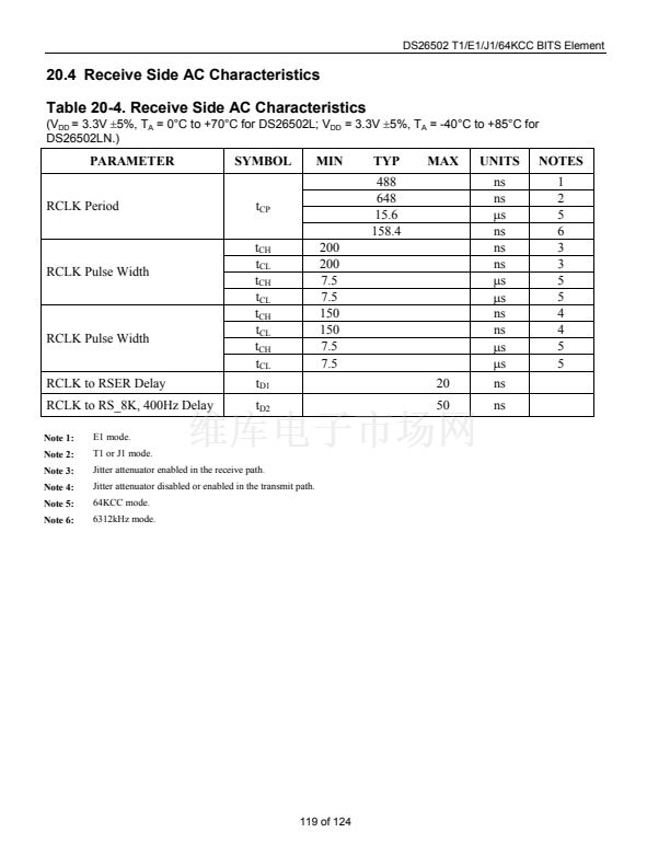
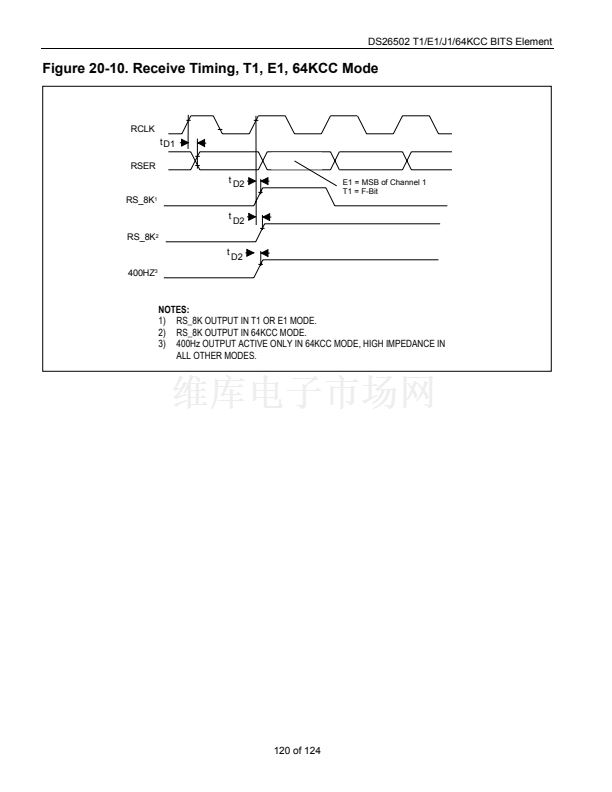
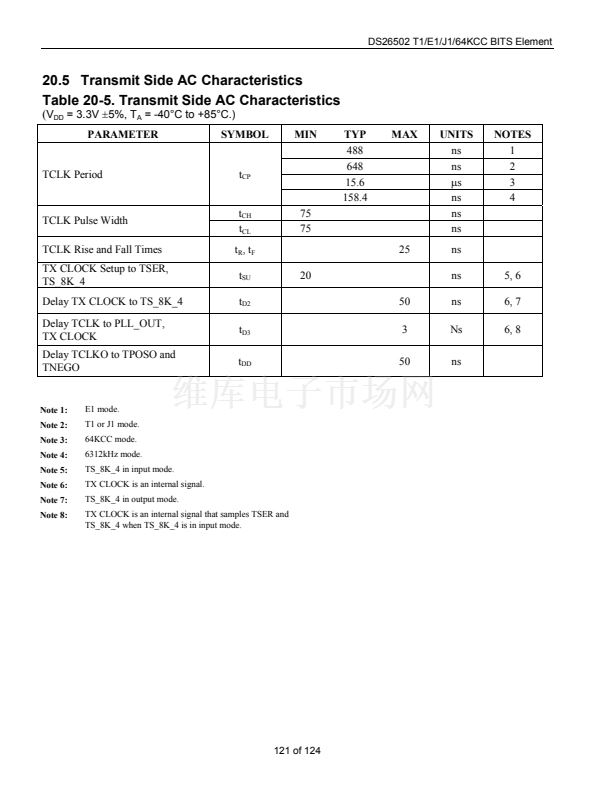
DS26502 T1/E1/J1/64KCC BITS Element
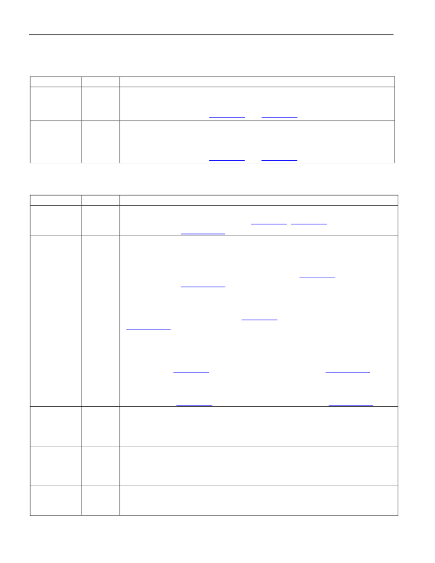
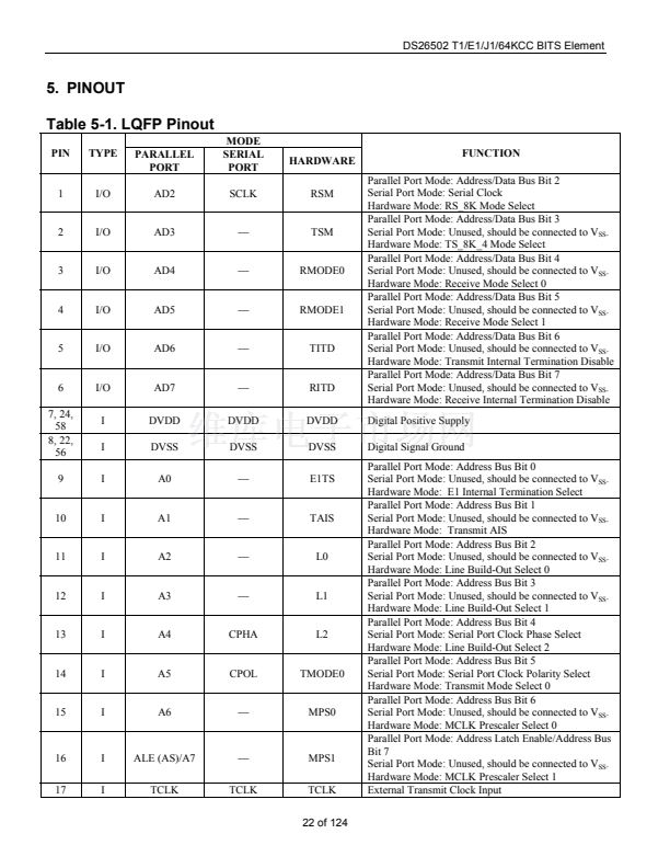
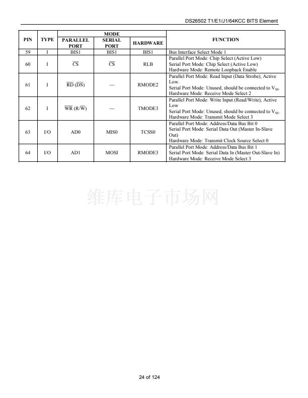
4. PIN FUNCTION DESCRIPTION
4.1 Transmit PLL
NAME
PLL_OUT
TYPE
O
FUNCTION
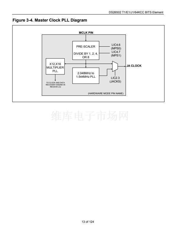
Transmit PLL Output.
This pin can be selected to output the 1544kHz,
2048kHz, 64kHz, or 6312kHz output from the internal TX PLL or the internal
signal, TX CLOCK. See
Figure 3-3
and
Figure 3-4.
Transmit Clock Input.
A 64kHz, 1.544MHz, 2.048MHz, or 6312kHz
primary clock. May be selected by the TX PLL mux to either directly drive
the transmit section or be converted to one of the other rates prior to driving
the transmit section. See
Figure 3-3
and
Figure 3-4.
TCLK
I
4.2 Transmit Side
NAME
TSER
TYPE
I
FUNCTION
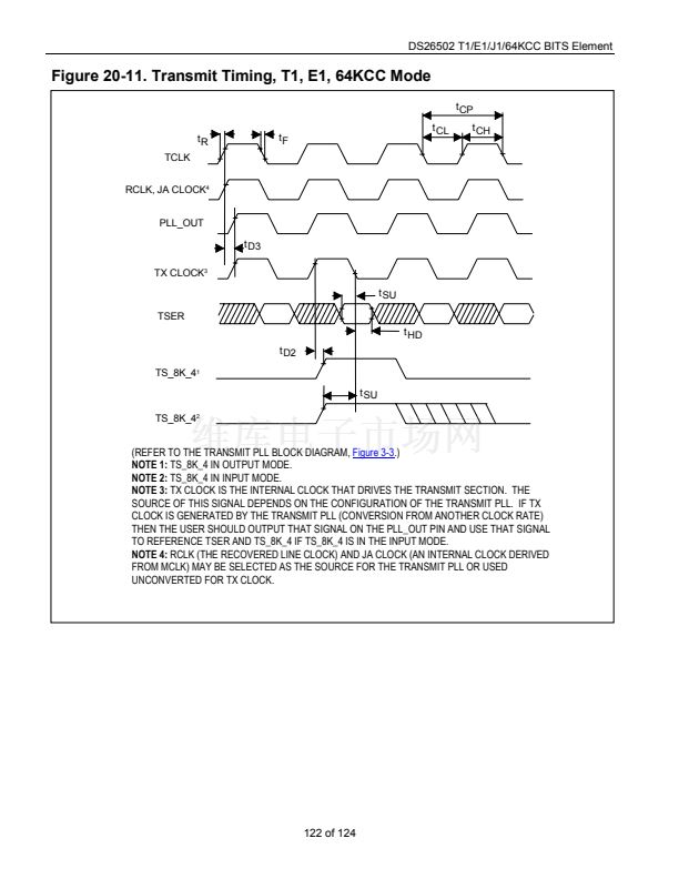
Transmit Serial Data.
Source of transmit data sampled on the falling edge of
TX CLOCK (an internal signal). See
Figure 3-1, Figure 3-3,
and the transmit
timing diagram (Figure
20-11).
TSYNC, 8kHz Sync, 400Hz Sync
T1/E1 Mode:
In input mode, this pin is sampled on the falling edge of TX
CLOCK (an internal signal) and a pulse at this pin will establish either frame
or multiframe boundaries for the transmit side. See
Figure 3-1
and the transmit
timing diagram (Figure
20-11).
In output mode, this pin is updated on the rising edge of TX CLOCK (an
internal signal) and can be programmed to output a frame or multiframe sync
pulse useful for aligning data. See
Figure 3-1
and the transmit timing diagram
(Figure
20-11).
64KCC Mode:
In input mode, this pin is sampled on the falling edge of TX
CLOCK (an internal signal) and will establish the boundary for the 8kHz
portion of the Composite Clock or the 400Hz boundary based on the setting of
IOCR1.3. See
Figure 3-1
and the transmit timing diagram (Figure
20-11).
In output mode, this pin is updated on the rising edge of TX CLOCK (an
internal signal) and will indicate the 8kHz or 400Hz composite clock
alignment. See
Figure 3-1
and the transmit timing diagram (Figure
20-11).
Transmit Clock Output.
In normal operation this output is the selected
transmit clock from the TX_PLL, TCLK pin or the recovered clock (RCLK).
When remote loopback is enabled this pin will output the recovered network
clock.
Transmit Positive-Data Output.
In T1 or E1 mode, updated on the rising
edge of TCLKO with the bipolar data out of the transmit-side formatter. Can
be programmed to source NRZ data via the output-data format (IOCR1.0)
control bit. In 64KCC or 6312kHz mode this pin will be low.
Transmit Negative-Data Output.
In T1 or E1 mode, updated on the rising
edge of TCLKO with the bipolar data out of the transmit-side formatter. In
64KCC or 6312kHz mode this pin will be low.
14 of 124
TS_8K_4
I/O
TCLKO
O
TPOSO
O
TNEGO
O


 1
1
 2
2
 3
3
 4
4
 5
5
 6
6
 7
7
 8
8
 9
9
 10
10
 11
11
 12
12
 13
13
 14
14
 15
15
 16
16
 17
17
 18
18
 19
19
 20
20
 21
21
 22
22
 23
23
 24
24
 25
25
 26
26
 27
27
 28
28
 29
29
 30
30
 31
31
 32
32
 33
33
 34
34
 35
35
 36
36
 37
37
 38
38
 39
39
 40
40
 41
41
 42
42
 43
43
 44
44
 45
45
 46
46
 47
47
 48
48
 49
49
 50
50
 51
51
 52
52
 53
53
 54
54
 55
55
 56
56
 57
57
 58
58
 59
59
 60
60
 61
61
 62
62
 63
63
 64
64
 65
65
 66
66
 67
67
 68
68
 69
69
 70
70
 71
71
 72
72
 73
73
 74
74
 75
75
 76
76
 77
77
 78
78
 79
79
 80
80
 81
81
 82
82
 83
83
 84
84
 85
85
 86
86
 87
87
 88
88
 89
89
 90
90
 91
91
 92
92
 93
93
 94
94
 95
95
 96
96
 97
97
 98
98
 99
99
 100
100
 101
101
 102
102
 103
103
 104
104
 105
105
 106
106
 107
107
 108
108
 109
109
 110
110
 111
111
 112
112
 113
113
 114
114
 115
115
 116
116
 117
117
 118
118
 119
119
 120
120
 121
121
 122
122
 123
123
 124
124
