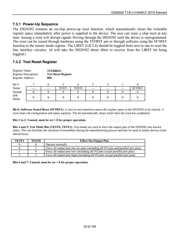
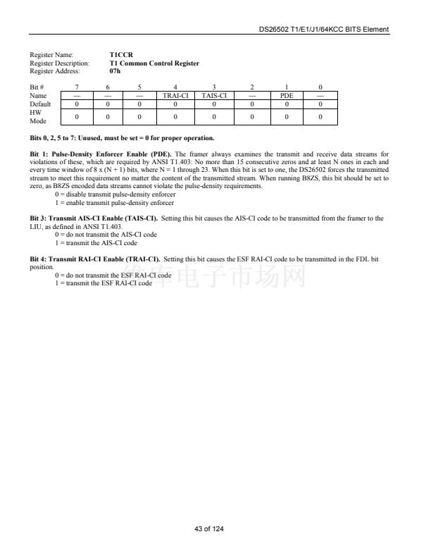
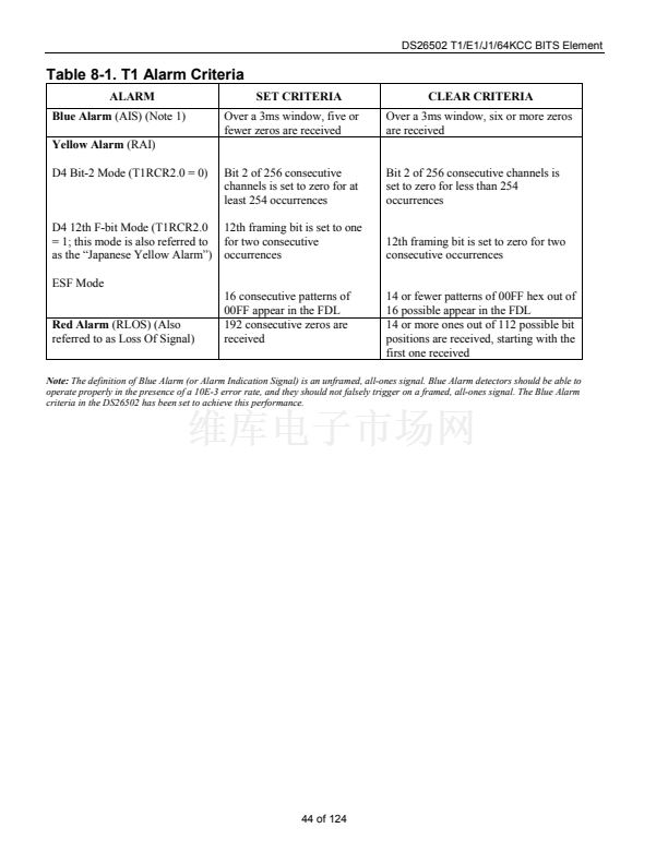
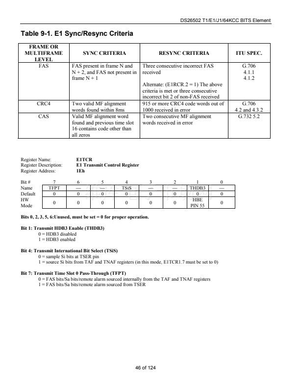
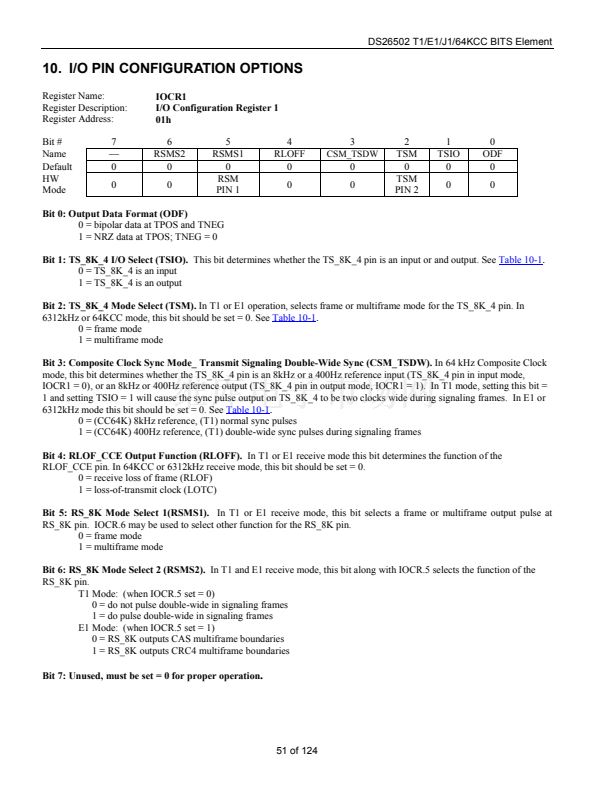
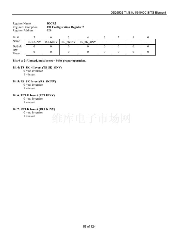
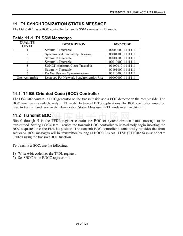
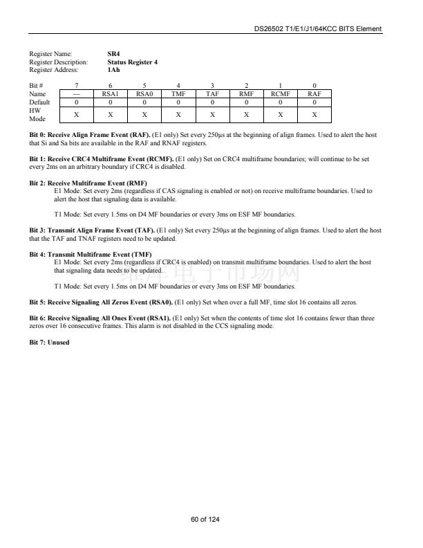
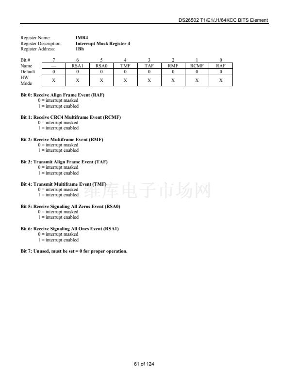
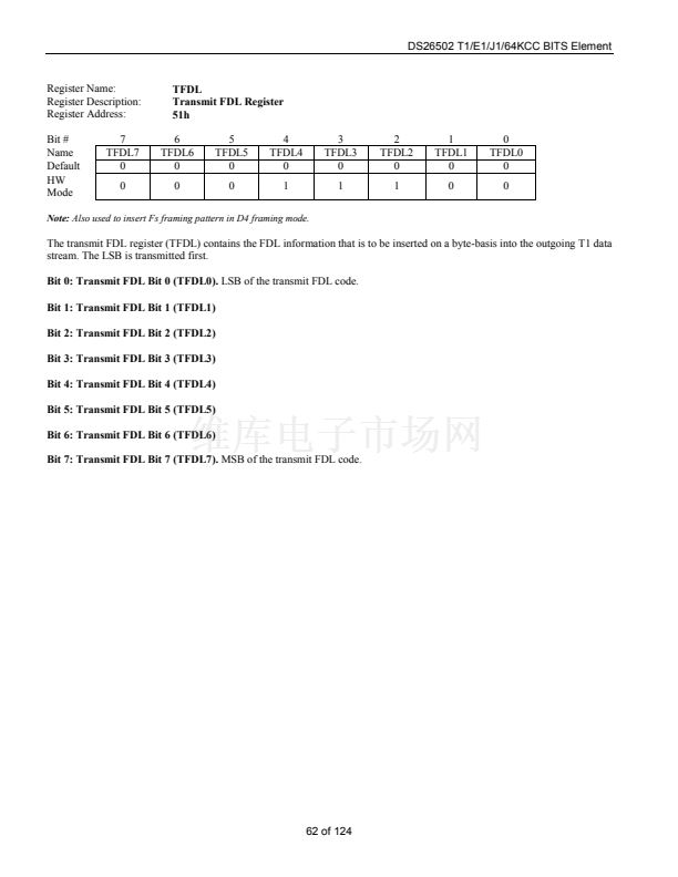
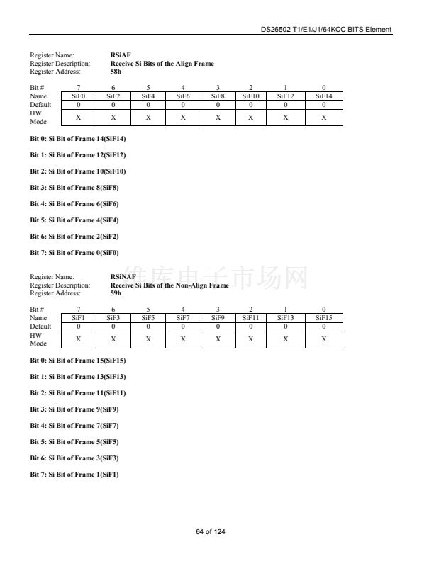
鈥?/div>
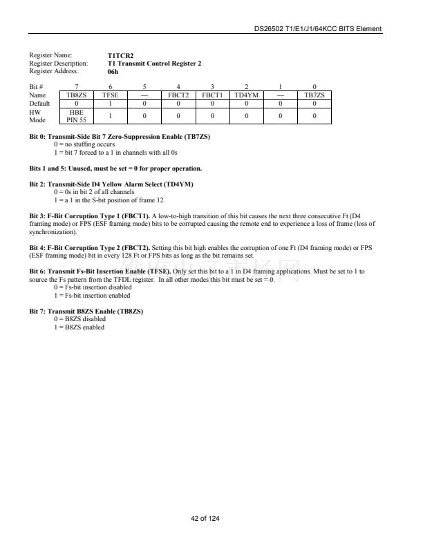
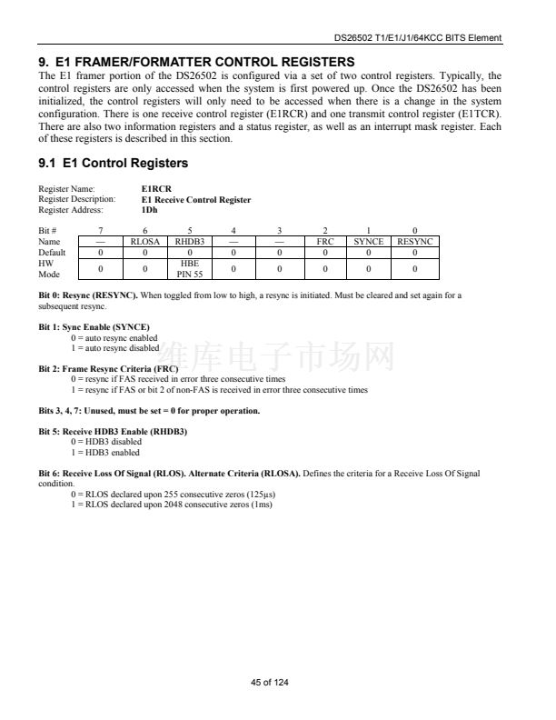
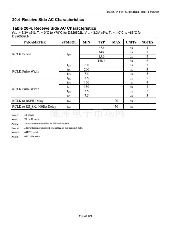
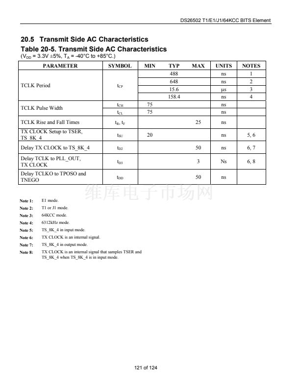
0
0
2
FRC
0
0
1
SYNCE
0
0
0
RESYNC
0
0
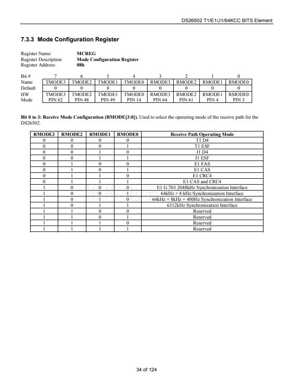
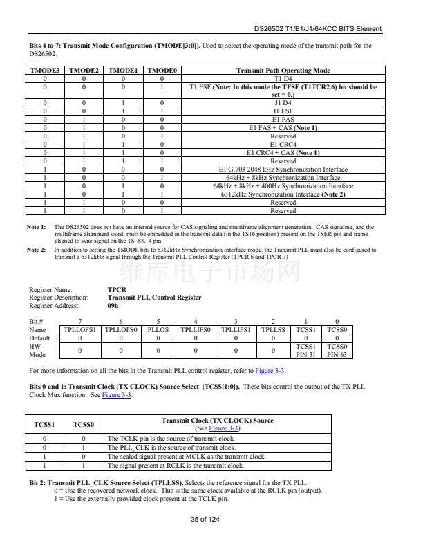
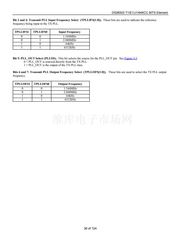
Bit 0: Resync (RESYNC).
When toggled from low to high, a resync is initiated. Must be cleared and set again for a
subsequent resync.
Bit 1: Sync Enable (SYNCE)
0 = auto resync enabled
1 = auto resync disabled
Bit 2: Frame Resync Criteria (FRC)
0 = resync if FAS received in error three consecutive times
1 = resync if FAS or bit 2 of non-FAS is received in error three consecutive times
Bits 3, 4, 7: Unused, must be set = 0 for proper operation.
Bit 5: Receive HDB3 Enable (RHDB3)
0 = HDB3 disabled
1 = HDB3 enabled
Bit 6: Receive Loss Of Signal (RLOS). Alternate Criteria (RLOSA).
Defines the criteria for a Receive Loss Of Signal
condition.
0 = RLOS declared upon 255 consecutive zeros (125碌s)
1 = RLOS declared upon 2048 consecutive zeros (1ms)
45 of 124


 1
1
 2
2
 3
3
 4
4
 5
5
 6
6
 7
7
 8
8
 9
9
 10
10
 11
11
 12
12
 13
13
 14
14
 15
15
 16
16
 17
17
 18
18
 19
19
 20
20
 21
21
 22
22
 23
23
 24
24
 25
25
 26
26
 27
27
 28
28
 29
29
 30
30
 31
31
 32
32
 33
33
 34
34
 35
35
 36
36
 37
37
 38
38
 39
39
 40
40
 41
41
 42
42
 43
43
 44
44
 45
45
 46
46
 47
47
 48
48
 49
49
 50
50
 51
51
 52
52
 53
53
 54
54
 55
55
 56
56
 57
57
 58
58
 59
59
 60
60
 61
61
 62
62
 63
63
 64
64
 65
65
 66
66
 67
67
 68
68
 69
69
 70
70
 71
71
 72
72
 73
73
 74
74
 75
75
 76
76
 77
77
 78
78
 79
79
 80
80
 81
81
 82
82
 83
83
 84
84
 85
85
 86
86
 87
87
 88
88
 89
89
 90
90
 91
91
 92
92
 93
93
 94
94
 95
95
 96
96
 97
97
 98
98
 99
99
 100
100
 101
101
 102
102
 103
103
 104
104
 105
105
 106
106
 107
107
 108
108
 109
109
 110
110
 111
111
 112
112
 113
113
 114
114
 115
115
 116
116
 117
117
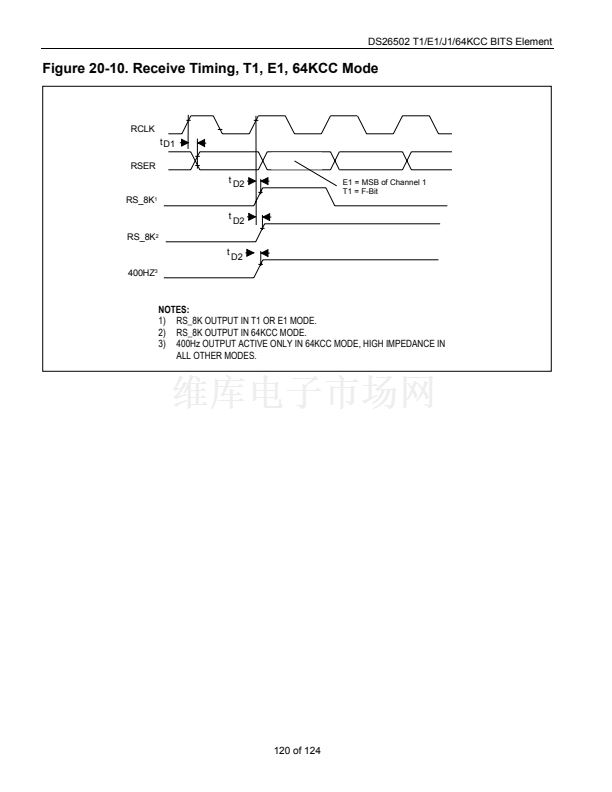
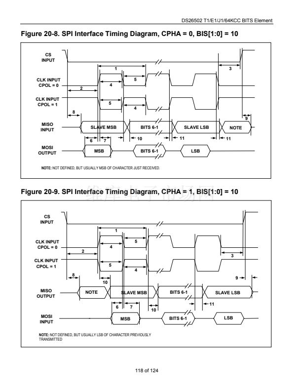 118
118
 119
119
 120
120
 121
121
 122
122
 123
123
 124
124
