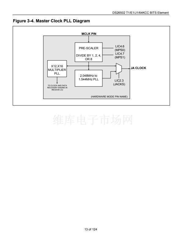
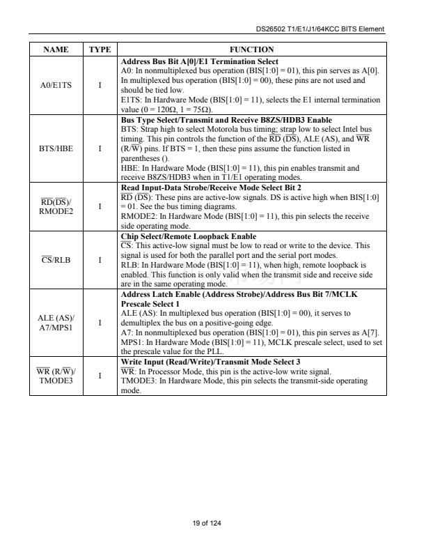
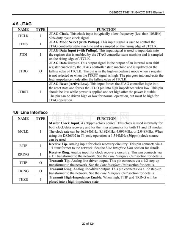
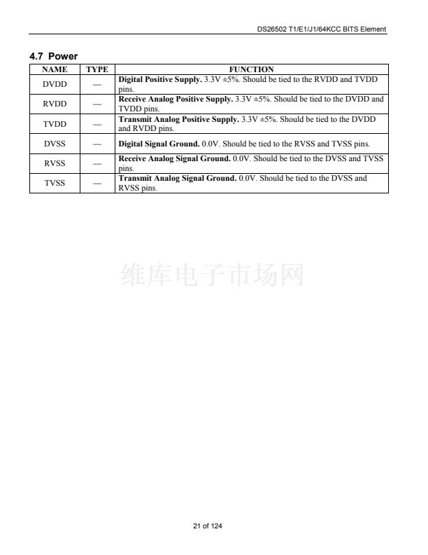
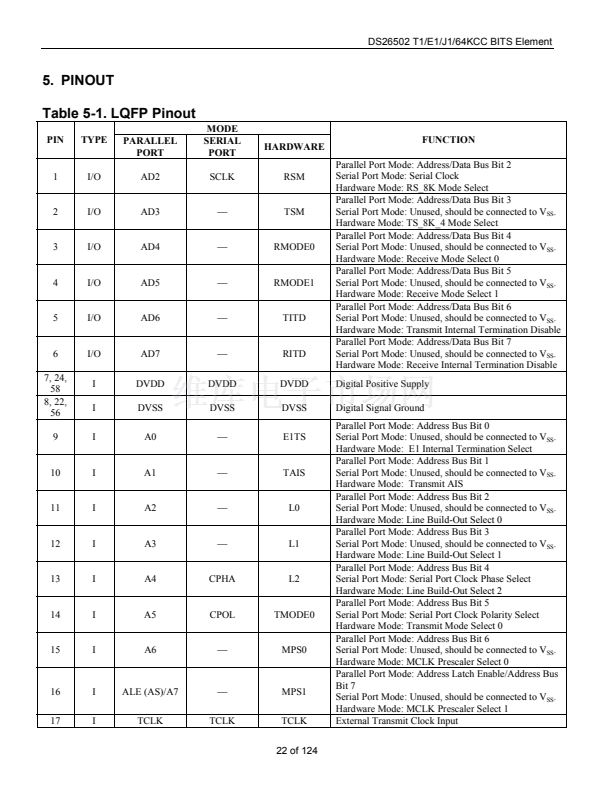
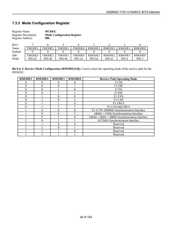
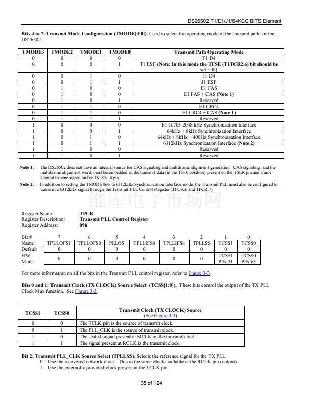
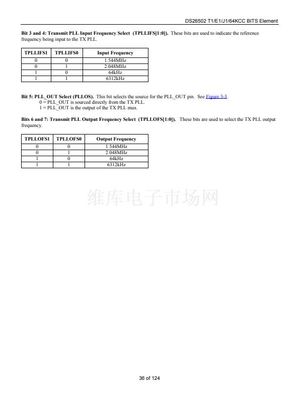
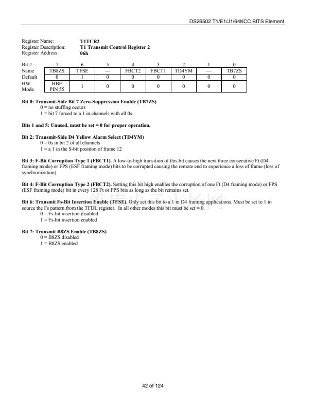
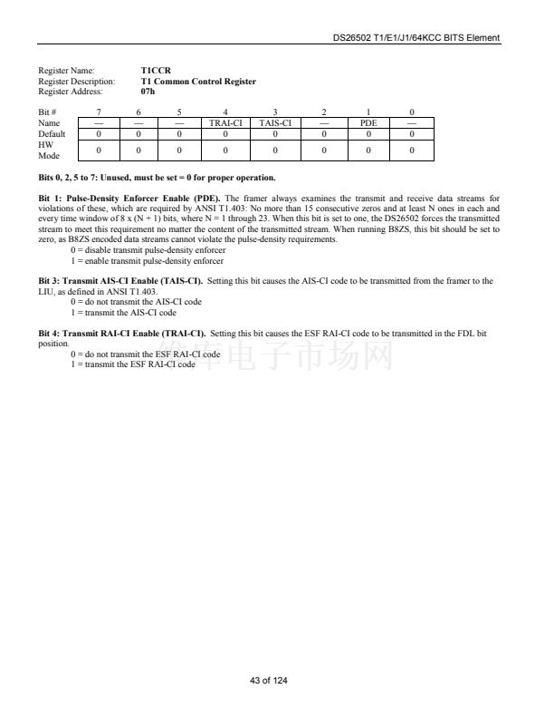
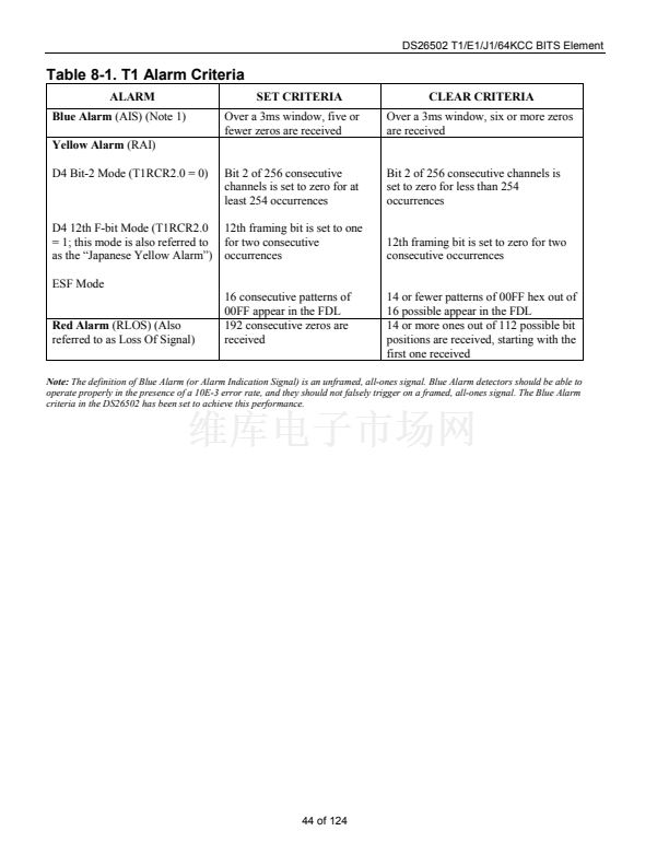
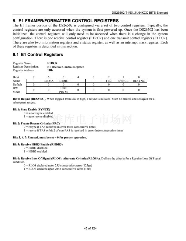
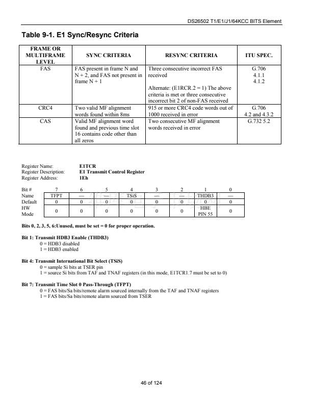
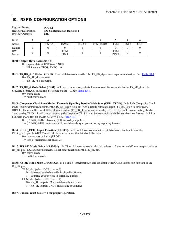
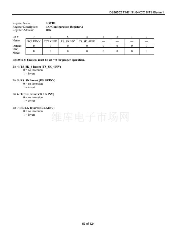
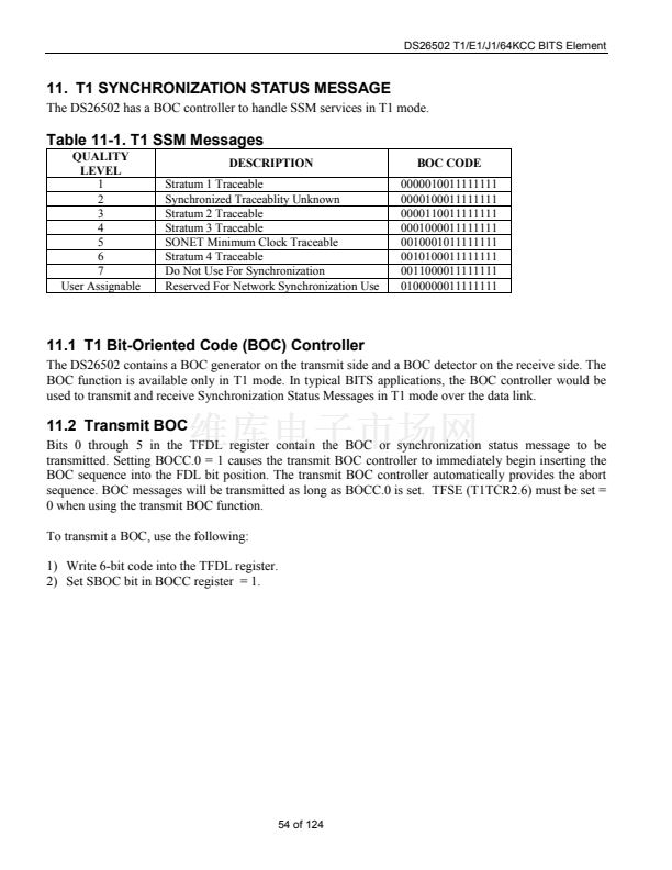
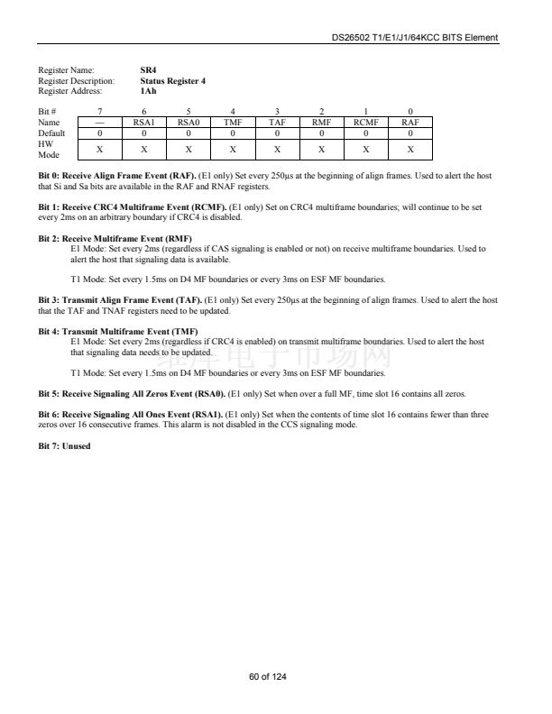
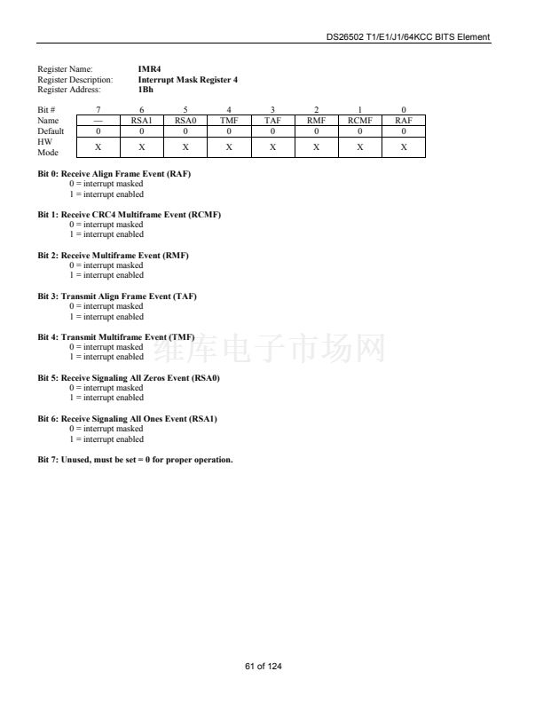
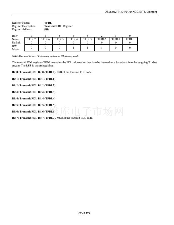
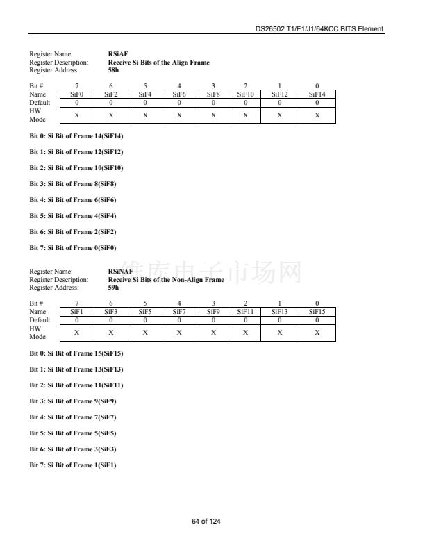
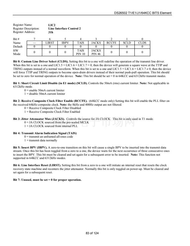
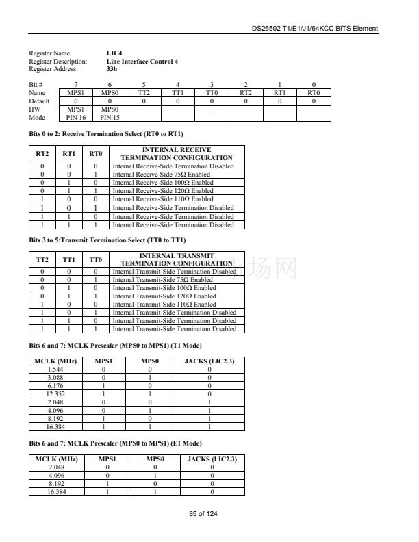
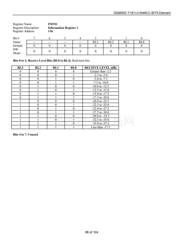
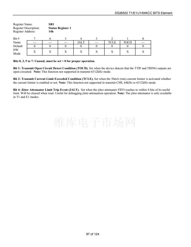
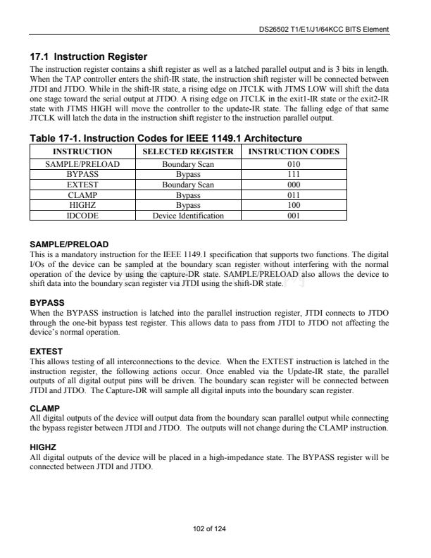
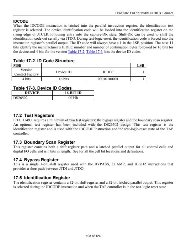
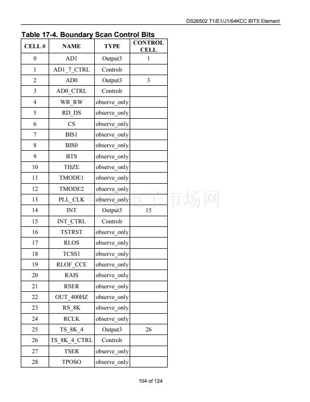
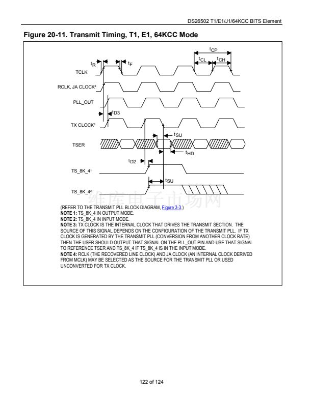
DS26502 T1/E1/J1/64KCC BITS Element
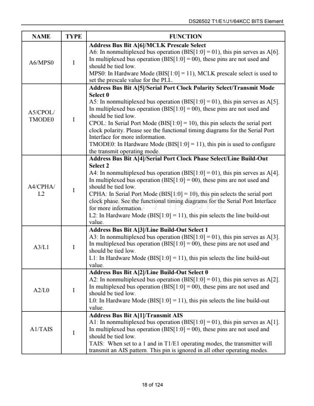
NAME
TYPE
AD[4]/
RMODE0
I/O
AD[3]/TSM
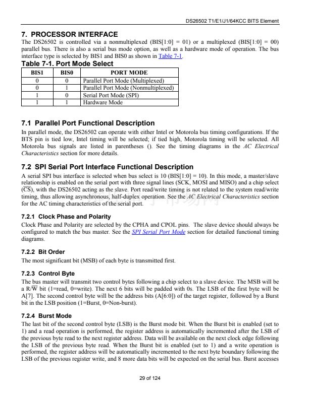
I/O
AD[2]/RSM/
SCLK
I/O
AD[1]/
RMODE3/
MOSI
I/O
AD[0]/
TCSS0/
MISO
I/O
FUNCTION
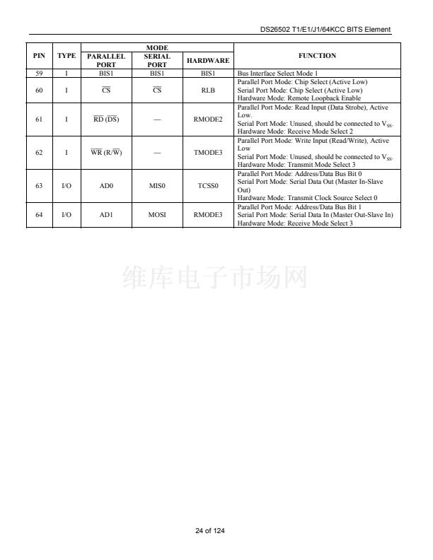
Data Bus D[4] or Address/Data Bus AD[4]/Receive Framing Mode Select
Bit 0
A[4]: In nonmultiplexed bus operation (BIS[1:0] = 01), it serves as the data
bus D[4].
AD[4]: In multiplexed bus operation (BIS[1:0] = 00), it serves as the
multiplexed address/data bus AD[4].
RMODE0: In Hardware Mode (BIS[1:0] = 11), it selects the receive side
operating mode.
Data Bus D[3] or Address/Data Bus AD[3]/TS_8K_4 Mode Select
A[3]: In nonmultiplexed bus operation (BIS[1:0] = 01), it serves as the data
bus D[3].
AD[3]: In multiplexed bus operation (BIS[1:0] = 00), it serves as the
multiplexed address/data bus AD[3].
TSM: In Hardware Mode (BIS[1:0] = 11), this pin selects the function of
TS_8K_4. Please see the register descriptions for more detailed information.
Data Bus D[2] or Address/Data Bus AD[2]/RS_8K Mode Select/
Serial Clock
A[2]: In nonmultiplexed bus operation (BIS[1:0] = 01), it serves as the data
bus D[2].
AD[2]: In multiplexed bus operation (BIS[1:0] = 00), it serves as the
multiplexed address/data bus AD[2].
RSM: In Hardware Mode (BIS[1:0] = 11), this pin selects the function of
RS_8K. Please see the register descriptions for more detailed information.
SCLK: In Serial Port mode this is the serial clock input.
Data Bus D[1] or Address/Data Bus AD[1]/Receive Mode Select 3/Master
Out-Slave In
A[1]: In nonmultiplexed bus operation (BIS[1:0] = 01), it serves as the data
bus D[1].
AD[1]: In multiplexed bus operation (BIS[1:0] = 00), it serves as the
multiplexed address/data bus AD[1].
RMODE3: In Hardware Mode (BIS[1:0] = 11), this pin selects the receive
side operating mode.
MOSI: Serial data input called Master Out-Slave In for clarity of data transfer
direction.
Data Bus D[0] or Address/Data Bus AD[0]/Transmit Clock Source
Select 0/Master In-Slave Out
A[0]: In nonmultiplexed bus operation (BIS[1:0] = 01), it serves as the data
bus D[0].
AD[0]: In multiplexed bus operation (BIS[1:0] = 00), it serves as the
multiplexed address/data bus AD[0].
TCSS0: Transmit Clock Source Select 0.
MISO: In serial bus mode (BIS[1:0] = 10), this pin serves as the serial data
output Master In-Slave Out.
Transmit Clock Source Select.
Transmit Clock Source Select 1
TCSS1
I
17 of 124


 1
1
 2
2
 3
3
 4
4
 5
5
 6
6
 7
7
 8
8
 9
9
 10
10
 11
11
 12
12
 13
13
 14
14
 15
15
 16
16
 17
17
 18
18
 19
19
 20
20
 21
21
 22
22
 23
23
 24
24
 25
25
 26
26
 27
27
 28
28
 29
29
 30
30
 31
31
 32
32
 33
33
 34
34
 35
35
 36
36
 37
37
 38
38
 39
39
 40
40
 41
41
 42
42
 43
43
 44
44
 45
45
 46
46
 47
47
 48
48
 49
49
 50
50
 51
51
 52
52
 53
53
 54
54
 55
55
 56
56
 57
57
 58
58
 59
59
 60
60
 61
61
 62
62
 63
63
 64
64
 65
65
 66
66
 67
67
 68
68
 69
69
 70
70
 71
71
 72
72
 73
73
 74
74
 75
75
 76
76
 77
77
 78
78
 79
79
 80
80
 81
81
 82
82
 83
83
 84
84
 85
85
 86
86
 87
87
 88
88
 89
89
 90
90
 91
91
 92
92
 93
93
 94
94
 95
95
 96
96
 97
97
 98
98
 99
99
 100
100
 101
101
 102
102
 103
103
 104
104
 105
105
 106
106
 107
107
 108
108
 109
109
 110
110
 111
111
 112
112
 113
113
 114
114
 115
115
 116
116
 117
117
 118
118
 119
119
 120
120
 121
121
 122
122
 123
123
 124
124
