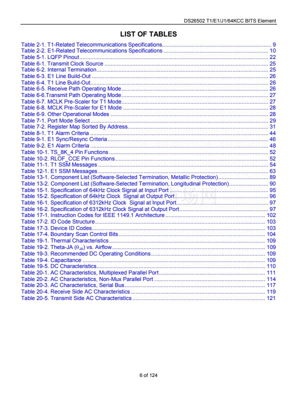
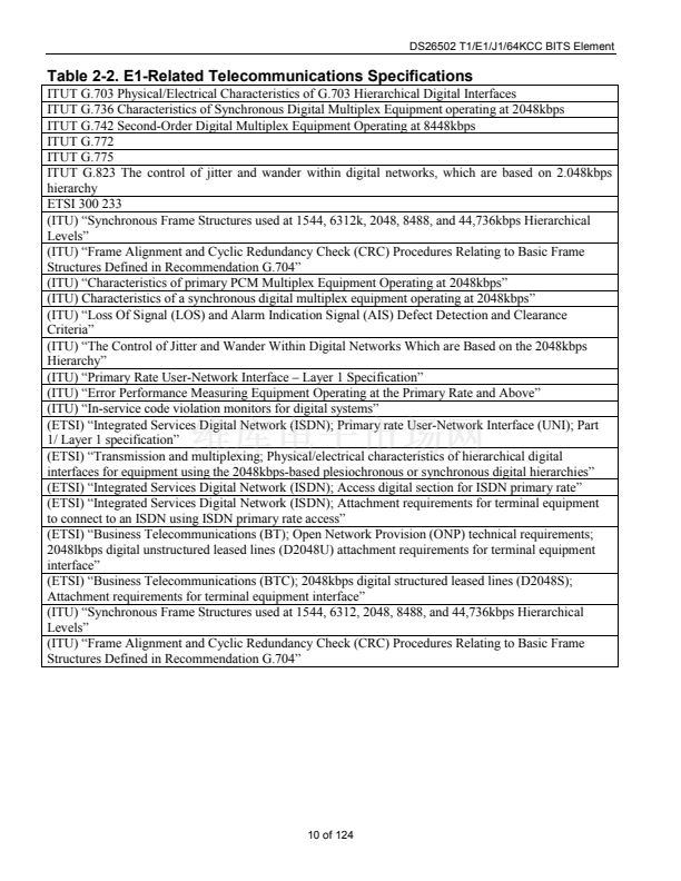
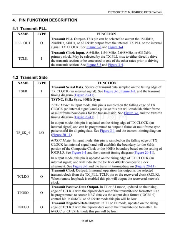
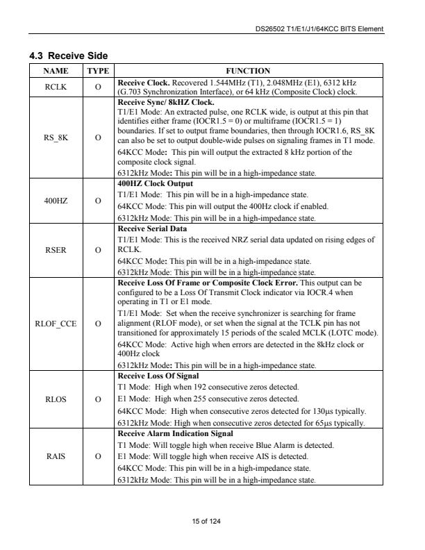
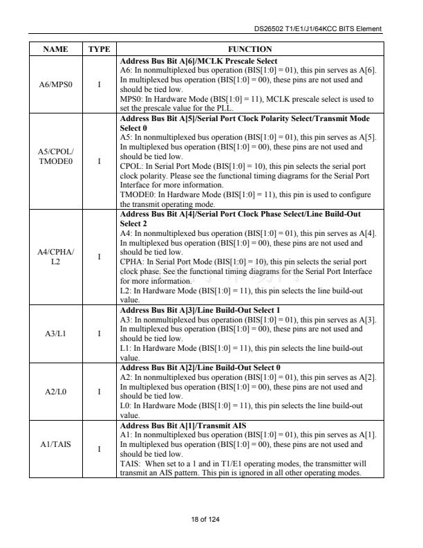
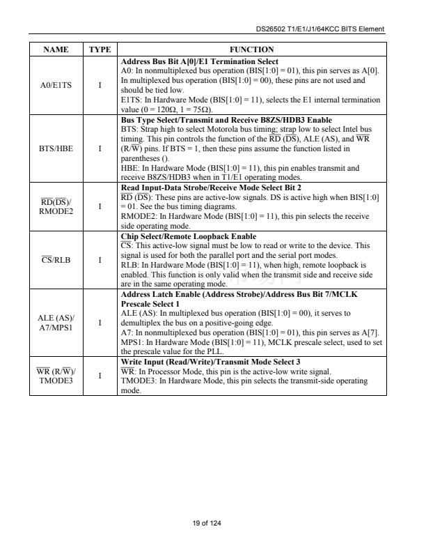
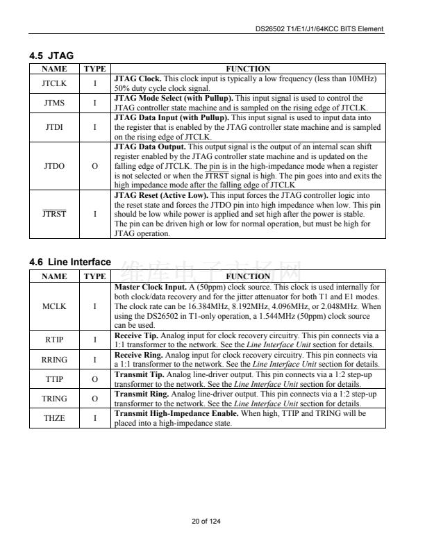
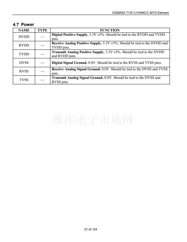
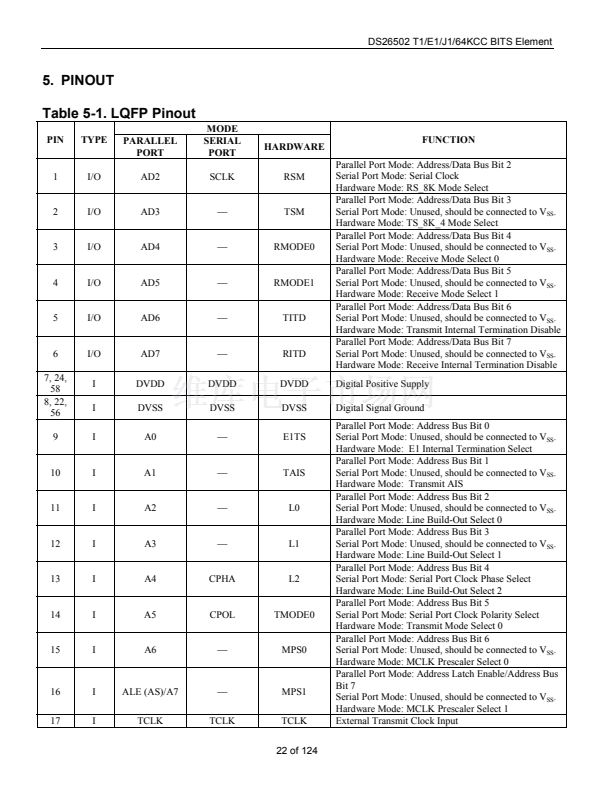
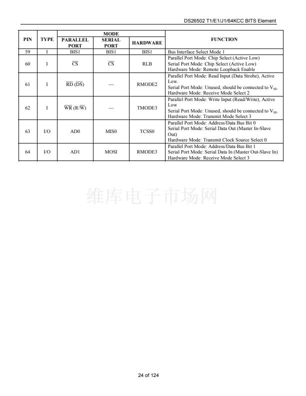
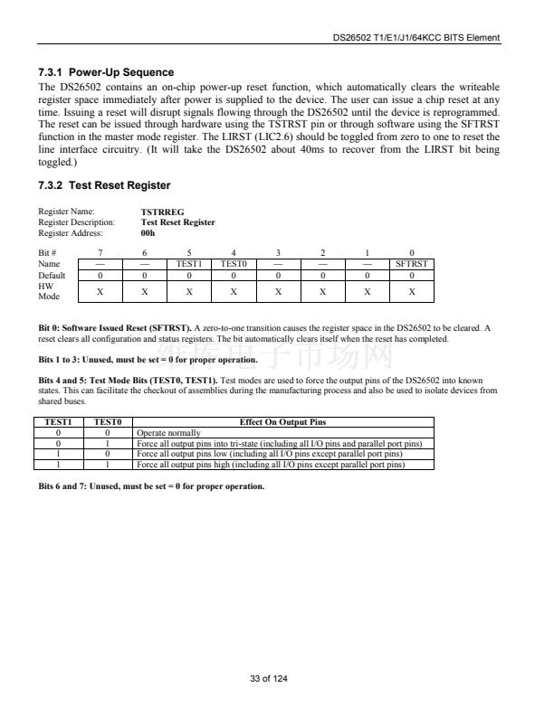
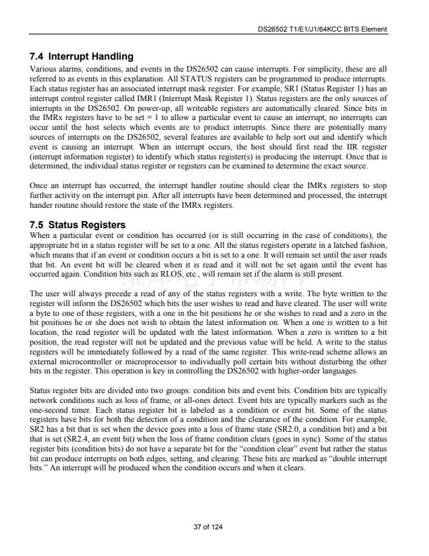
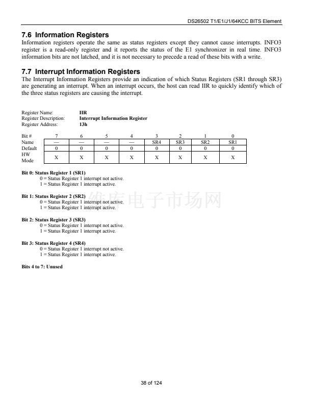
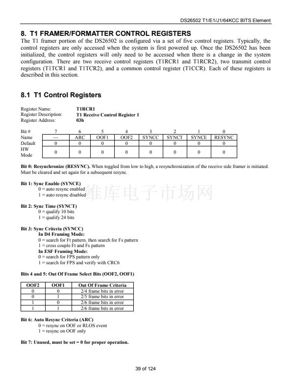
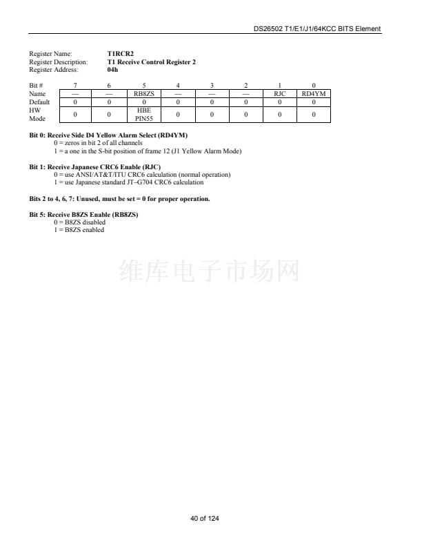
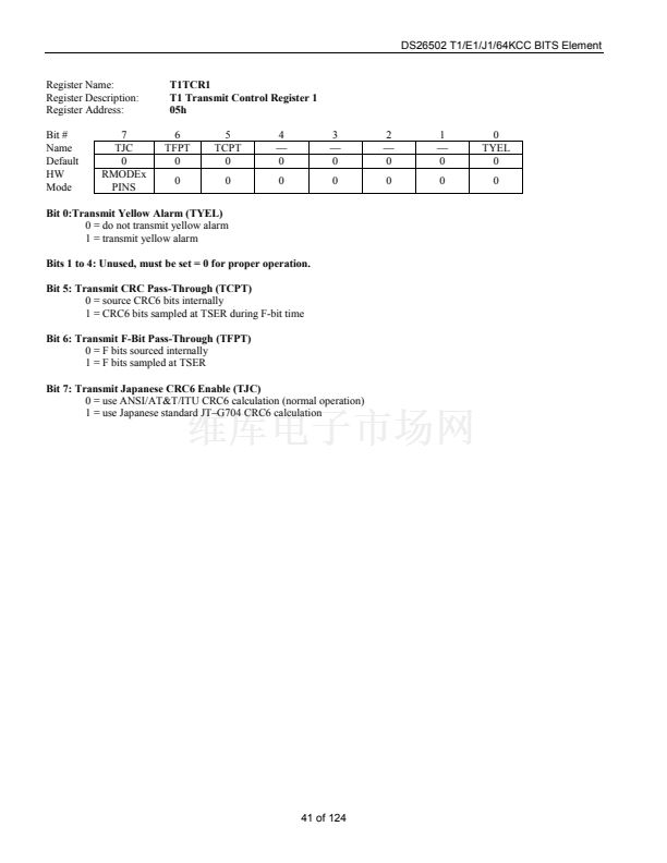
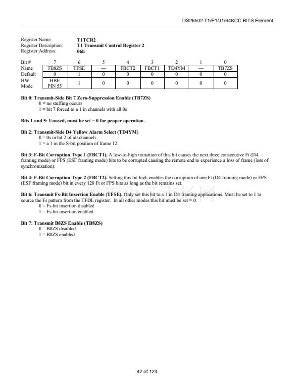
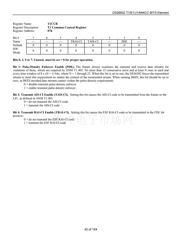
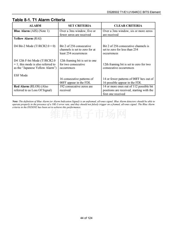
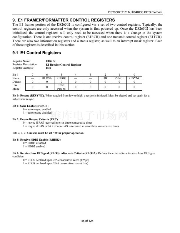
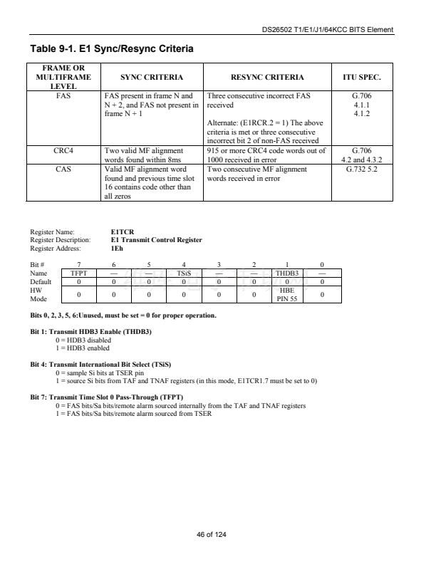
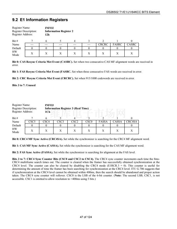
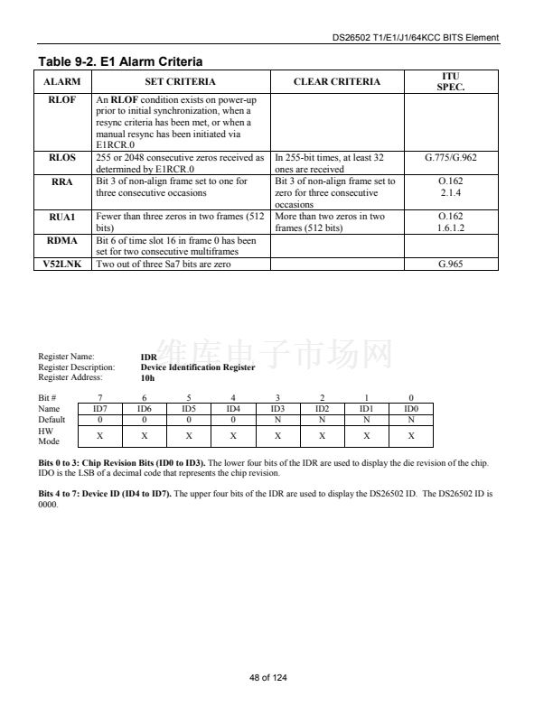
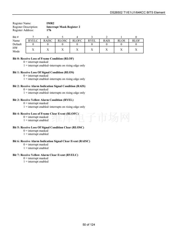
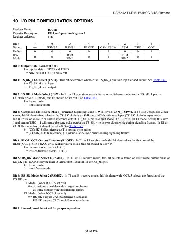
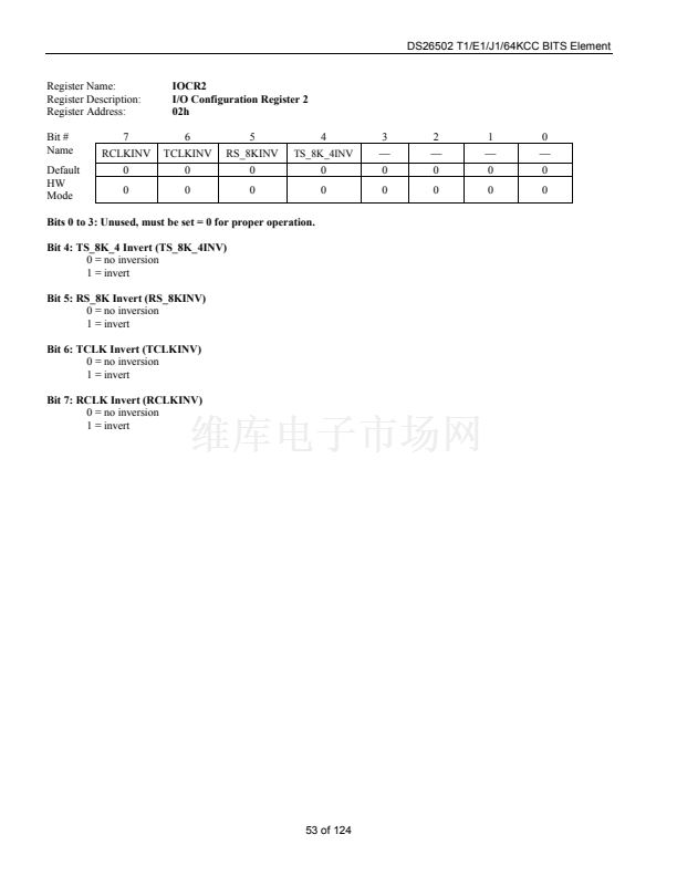
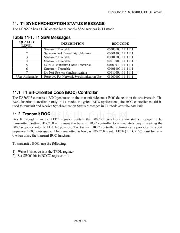
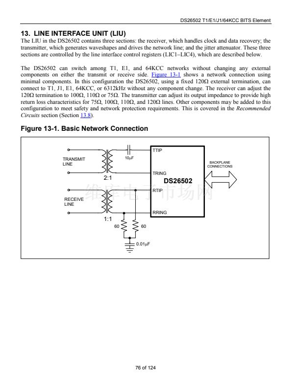
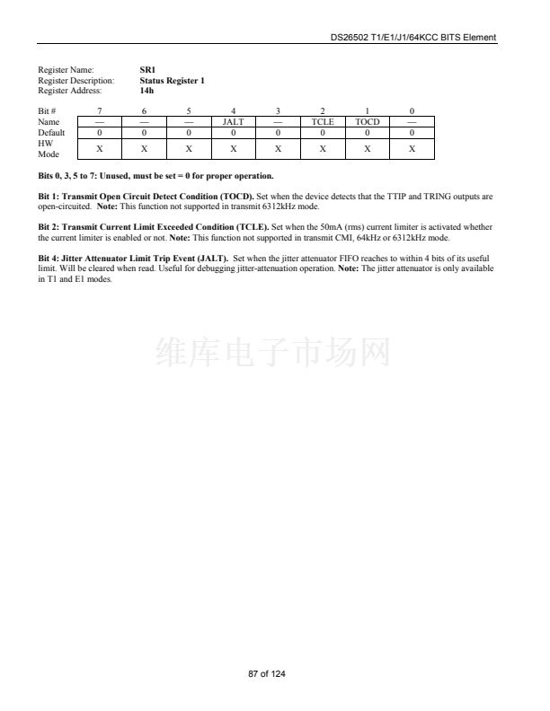
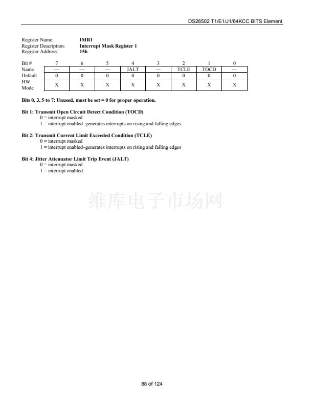
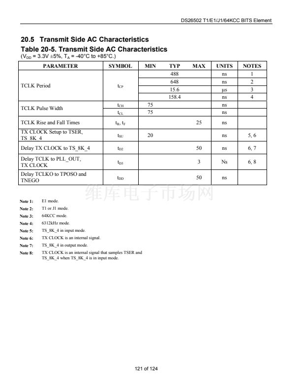
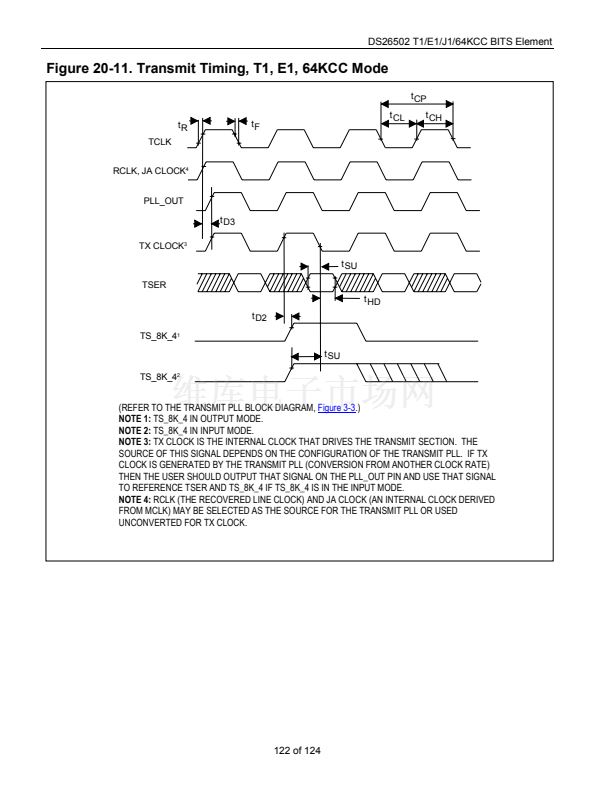
DS26502 T1/E1/J1/64KCC BITS Element
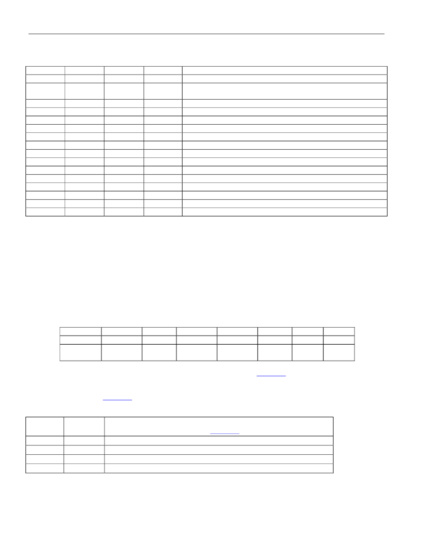
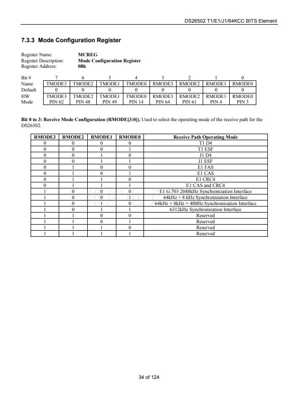
Bits 4 to 7: Transmit Mode Configuration (TMODE[3:0]).
Used to select the operating mode of the transmit path for the
DS26502.
TMODE3
0
0
0
0
0
0
0
0
0
0
1
1
1
1
1
1
Note 1:
TMODE2
0
0
0
0
1
1
1
1
1
1
0
0
0
0
1
1
TMODE1
0
0
1
1
0
0
0
1
1
1
0
0
1
1
0
0
TMODE0
0
1
0
1
0
0
1
0
0
1
0
1
0
1
0
1
Transmit Path Operating Mode
T1 D4
T1 ESF
(Note: In this mode the TFSE (T1TCR2.6) bit should be
set = 0.)
J1 D4
J1 ESF
E1 FAS
E1 FAS + CAS
(Note 1)
Reserved
E1 CRC4
E1 CRC4 + CAS
(Note 1)
Reserved
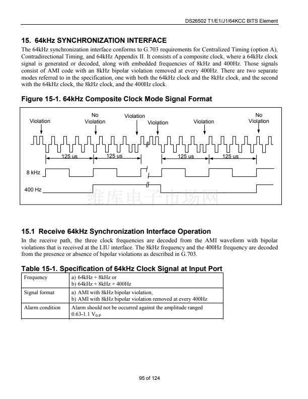
E1 G.703 2048 kHz Synchronization Interface
64kHz + 8kHz Synchronization Interface
64kHz + 8kHz + 400Hz Synchronization Interface
6312kHz Synchronization Interface
(Note 2)
Reserved
Reserved
Note 2:
The DS26502 does not have an internal source for CAS signaling and multiframe alignment generation. CAS signaling, and the
multiframe alignment word, must be embedded in the transmit data (in the TS16 position) present on the TSER pin and frame
aligned to sync signal on the TS_8K_4 pin.
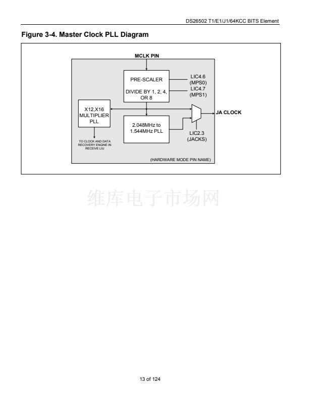
In addition to setting the TMODE bits to 6312kHz Synchronization Interface mode, the Transmit PLL must also be configured to
transmit a 6312kHz signal through the Transmit PLL Control Register (TPCR.6 and TPCR.7)
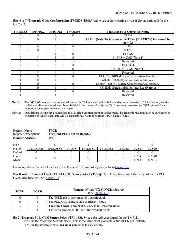
Register Name:
Register Description:
Register Address:
Bit #
Name
Default
HW
Mode
7
TPLLOFS1
0
0
TPCR
Transmit PLL Control Register
09h
6
TPLLOFS0
0
0
5
PLLOS
0
0
4
TPLLIFS0
0
0
3
TPLLIFS1
0
0
2
TPLLSS
0
0
1
TCSS1
0
TCSS1
PIN 31
0
TCSS0
0
TCSS0
PIN 63
For more information on all the bits in the Transmit PLL control register, refer to
Figure 3-3.
Bits 0 and 1: Transmit Clock (TX CLOCK) Source Select (TCSS[1:0]).
These bits control the output of the TX PLL
Clock Mux function. See
Figure 3-3.
TCSS1
0
0
1
1
TCSS0
0
1
0
1
Transmit Clock (TX CLOCK) Source
(See
Figure 3-3)
The TCLK pin is the source of transmit clock.
The PLL_CLK is the source of transmit clock.
The scaled signal present at MCLK as the transmit clock.
The signal present at RCLK is the transmit clock.
Bit 2: Transmit PLL_CLK Source Select (TPLLSS).
Selects the reference signal for the TX PLL.
0 = Use the recovered network clock. This is the same clock available at the RCLK pin (output).
1 = Use the externally provided clock present at the TCLK pin.
35 of 124


 1
1
 2
2
 3
3
 4
4
 5
5
 6
6
 7
7
 8
8
 9
9
 10
10
 11
11
 12
12
 13
13
 14
14
 15
15
 16
16
 17
17
 18
18
 19
19
 20
20
 21
21
 22
22
 23
23
 24
24
 25
25
 26
26
 27
27
 28
28
 29
29
 30
30
 31
31
 32
32
 33
33
 34
34
 35
35
 36
36
 37
37
 38
38
 39
39
 40
40
 41
41
 42
42
 43
43
 44
44
 45
45
 46
46
 47
47
 48
48
 49
49
 50
50
 51
51
 52
52
 53
53
 54
54
 55
55
 56
56
 57
57
 58
58
 59
59
 60
60
 61
61
 62
62
 63
63
 64
64
 65
65
 66
66
 67
67
 68
68
 69
69
 70
70
 71
71
 72
72
 73
73
 74
74
 75
75
 76
76
 77
77
 78
78
 79
79
 80
80
 81
81
 82
82
 83
83
 84
84
 85
85
 86
86
 87
87
 88
88
 89
89
 90
90
 91
91
 92
92
 93
93
 94
94
 95
95
 96
96
 97
97
 98
98
 99
99
 100
100
 101
101
 102
102
 103
103
 104
104
 105
105
 106
106
 107
107
 108
108
 109
109
 110
110
 111
111
 112
112
 113
113
 114
114
 115
115
 116
116
 117
117
 118
118
 119
119
 120
120
 121
121
 122
122
 123
123
 124
124
