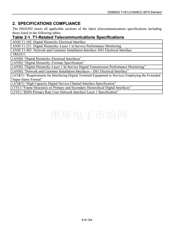
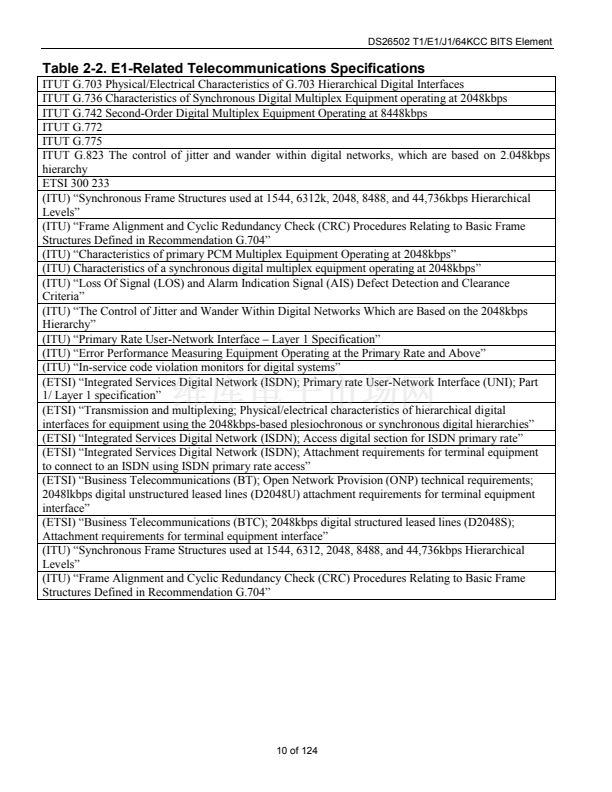
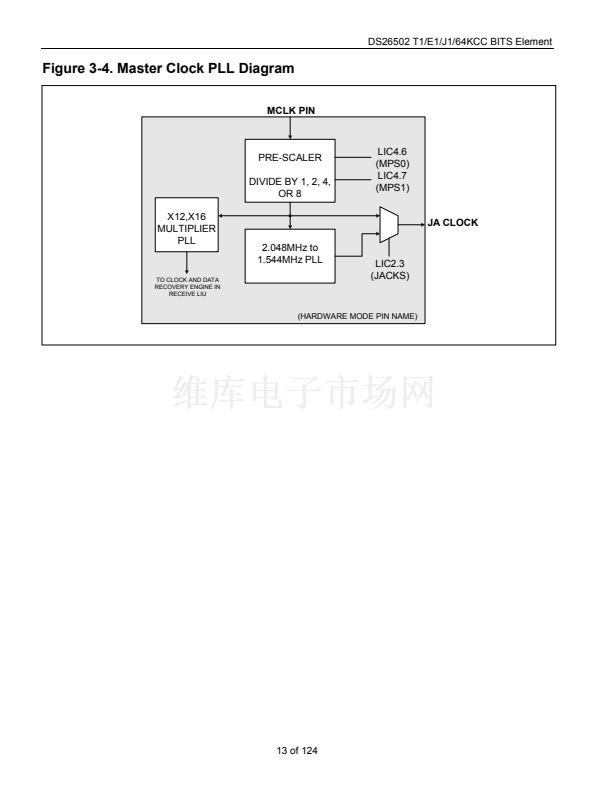
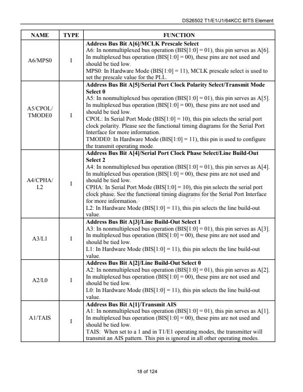
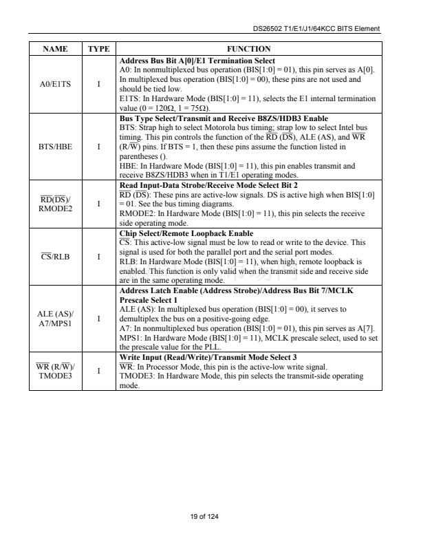
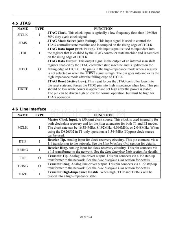
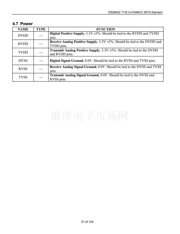
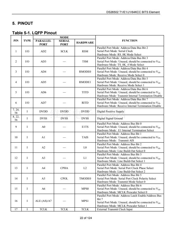
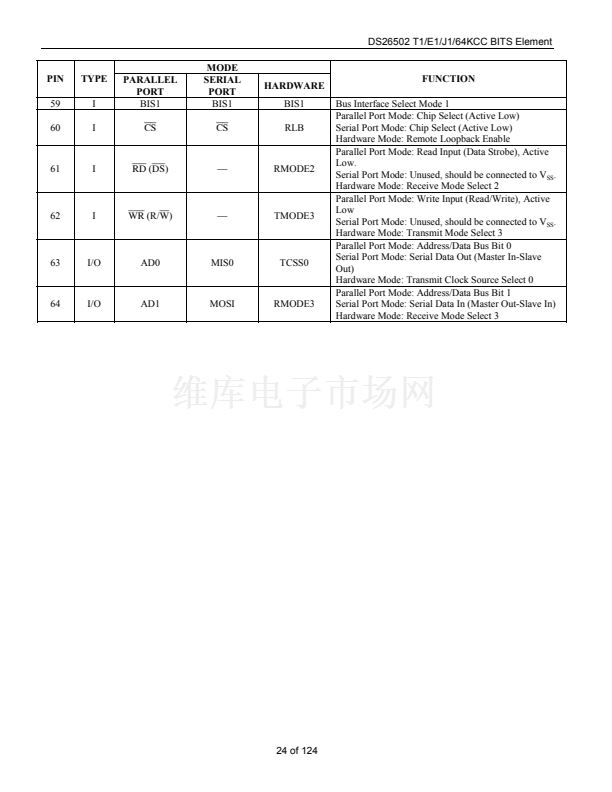
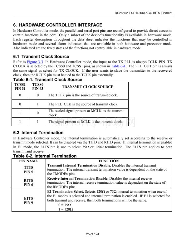
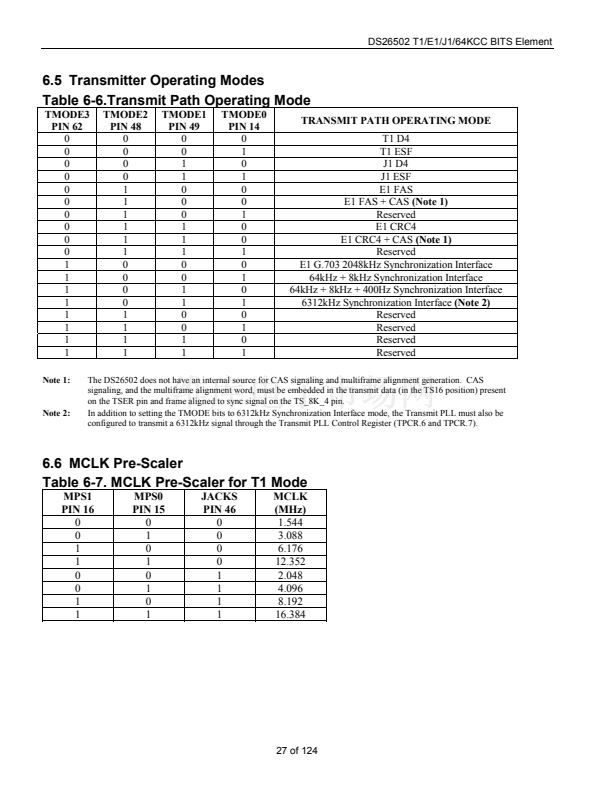
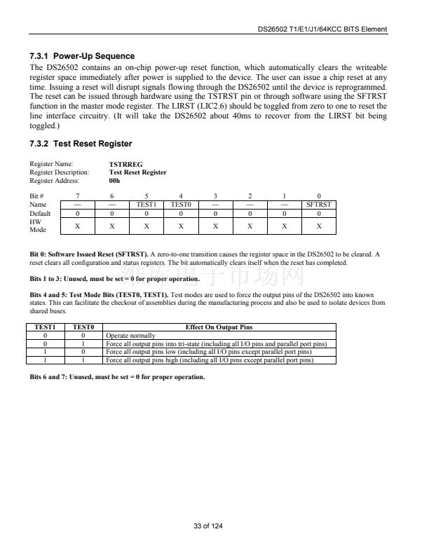
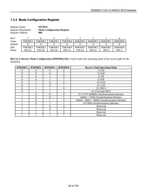
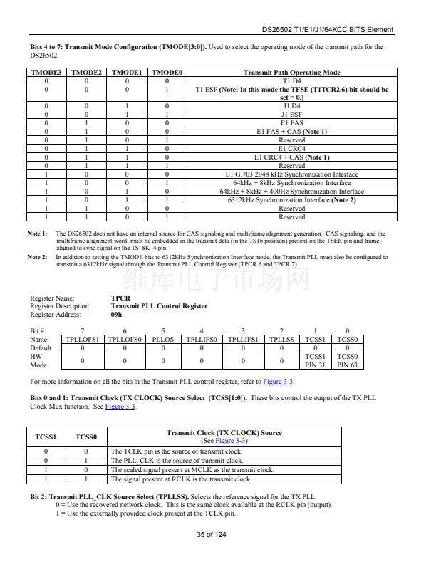
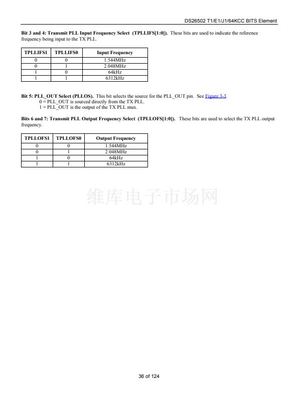
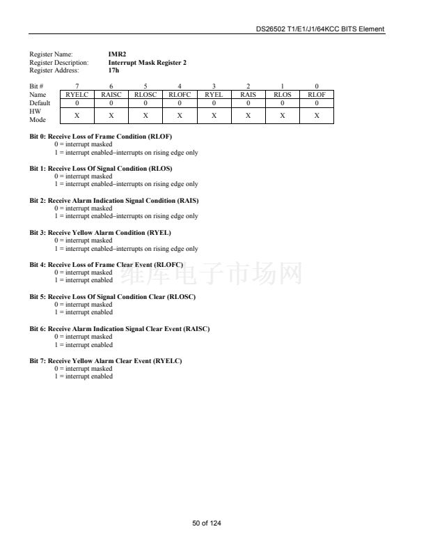
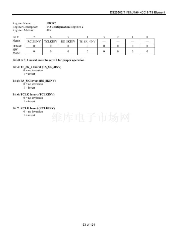
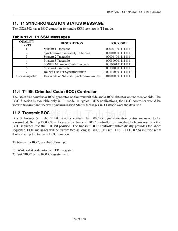
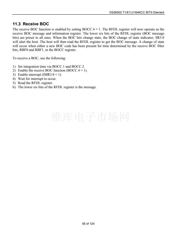
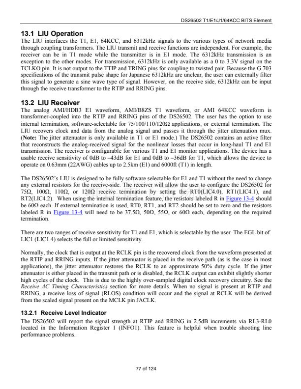
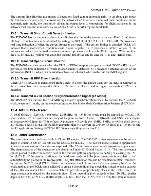
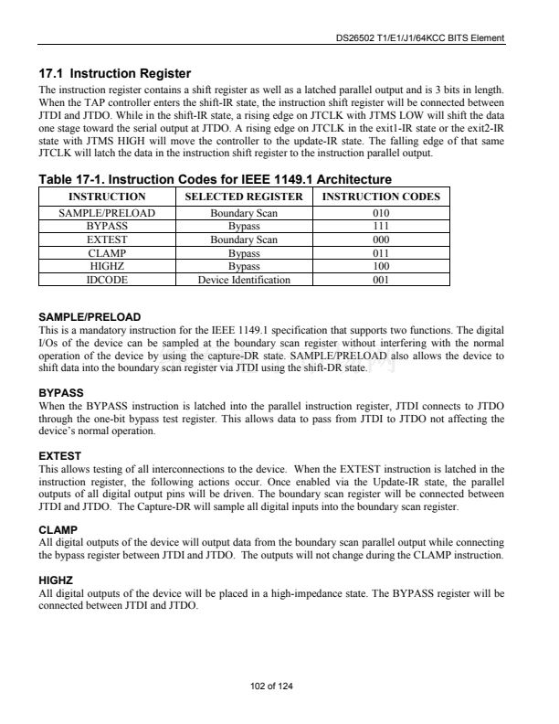
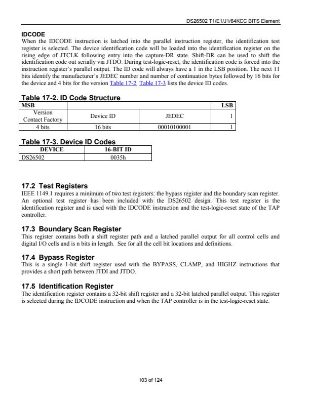
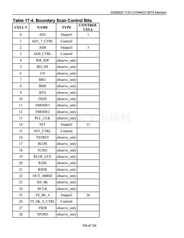
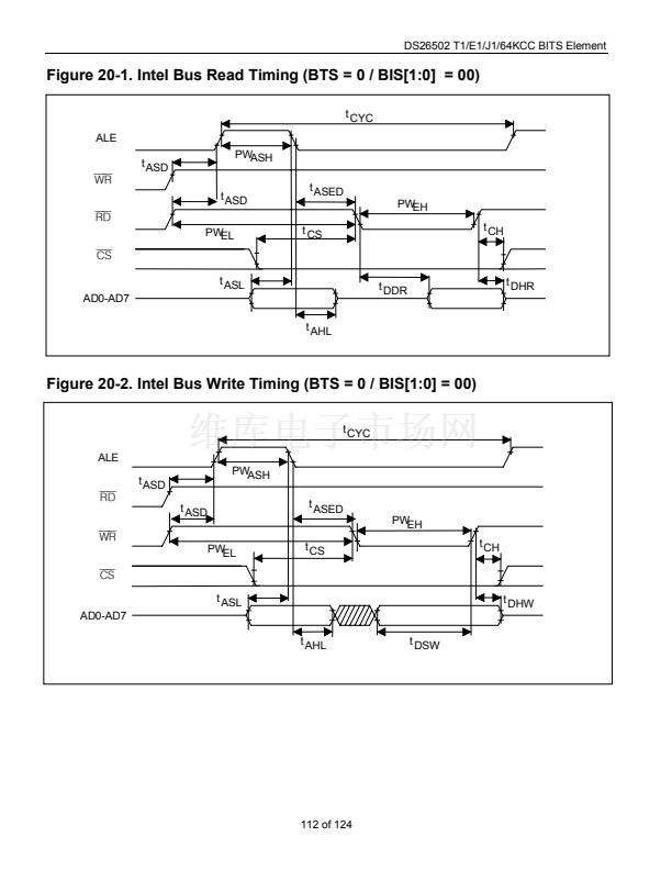
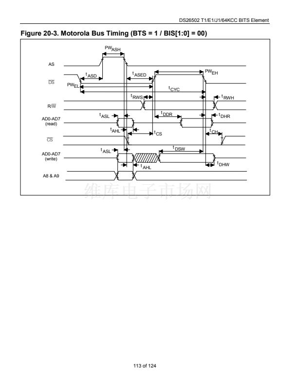
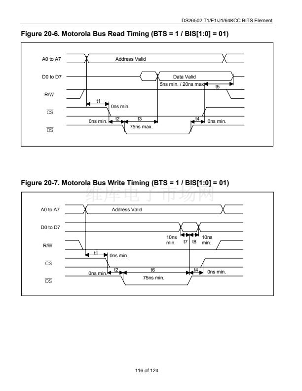
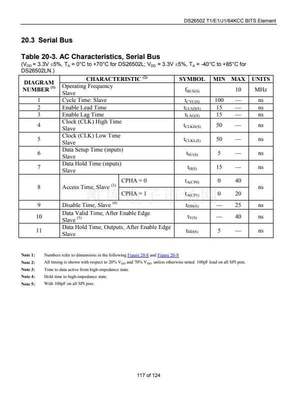
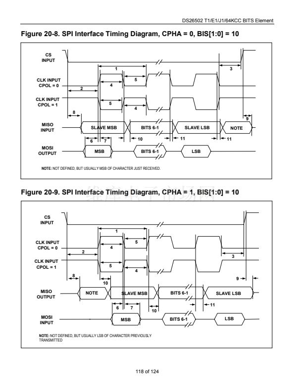
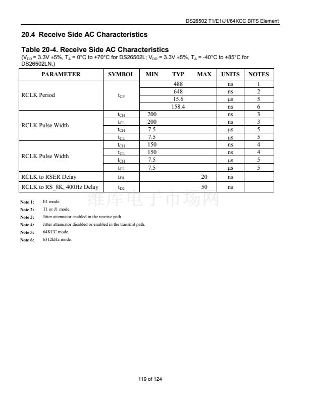
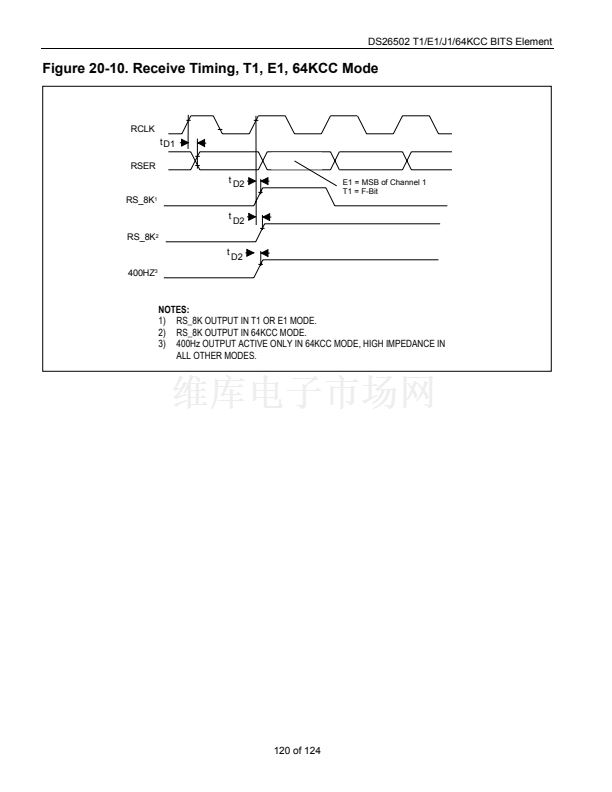
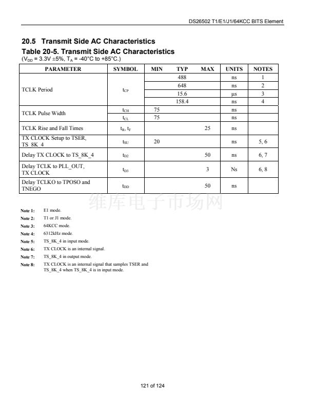
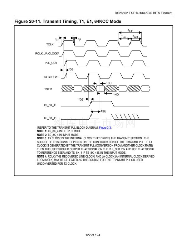
DS26502 T1/E1/J1/64KCC BITS Element
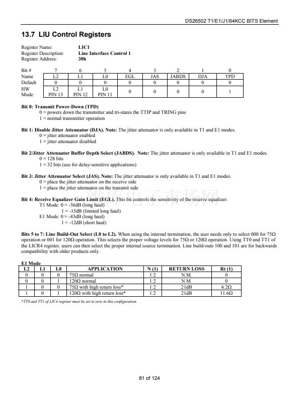
13.7 LIU Control Registers
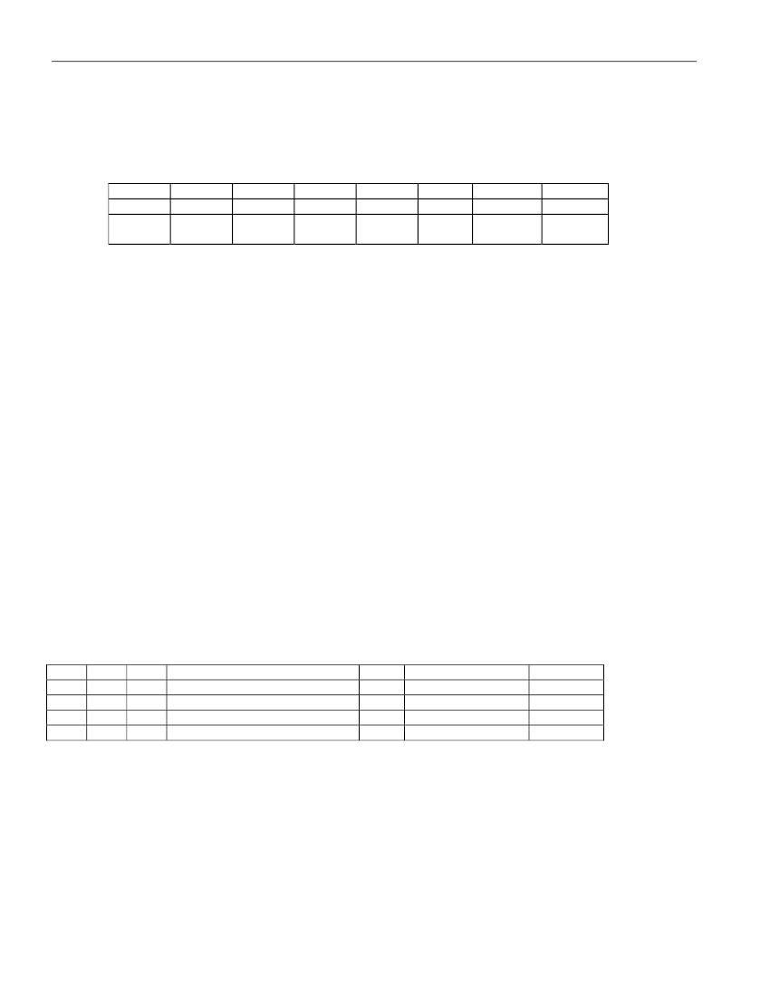
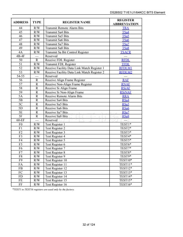
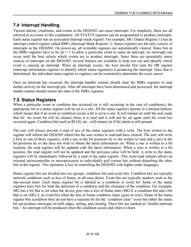
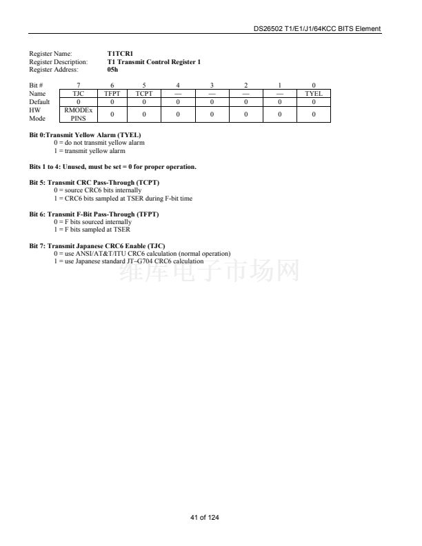
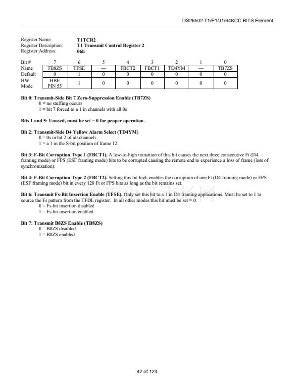
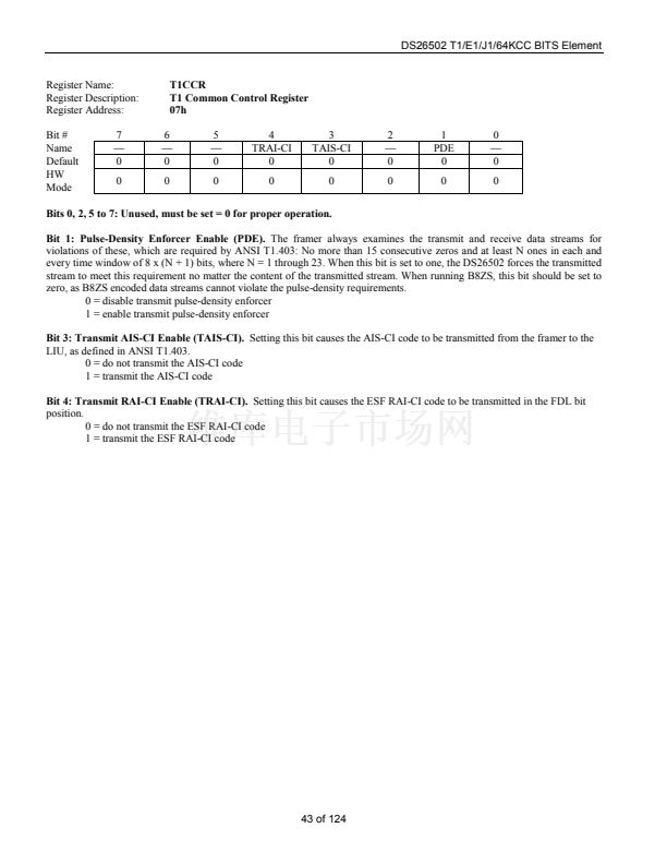
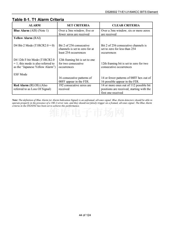
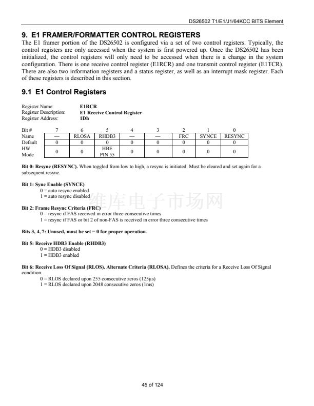
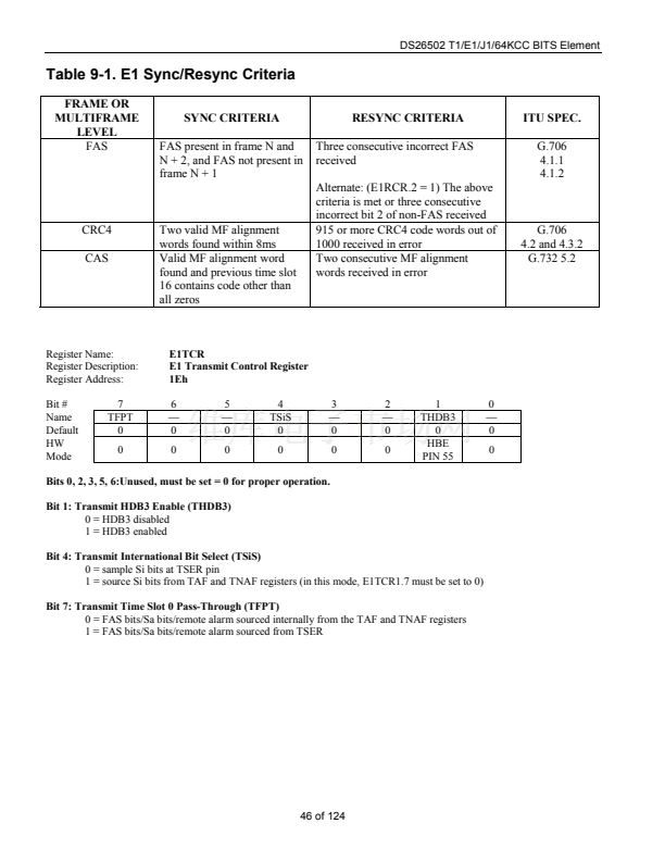
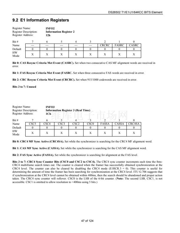
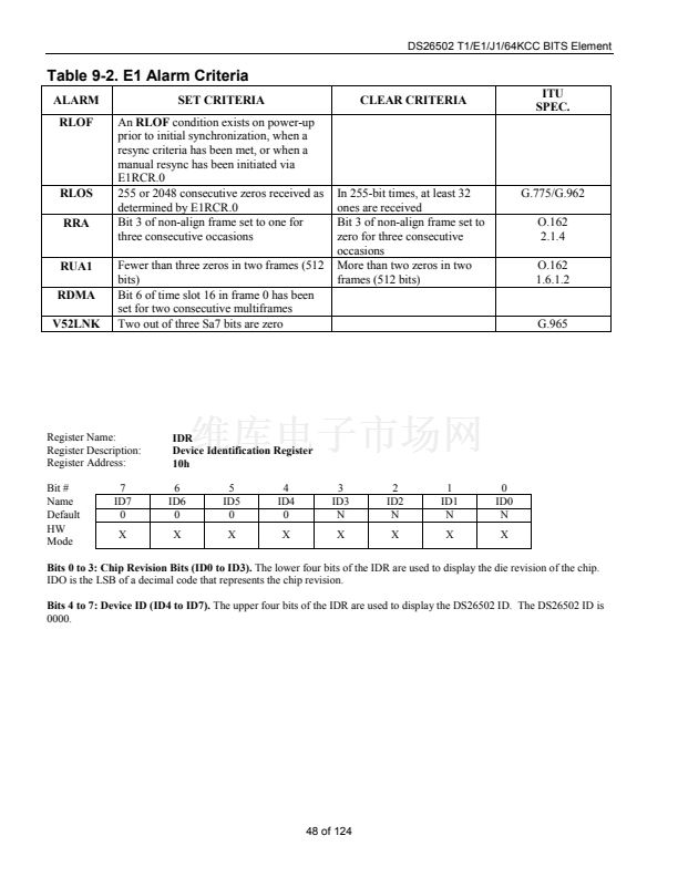
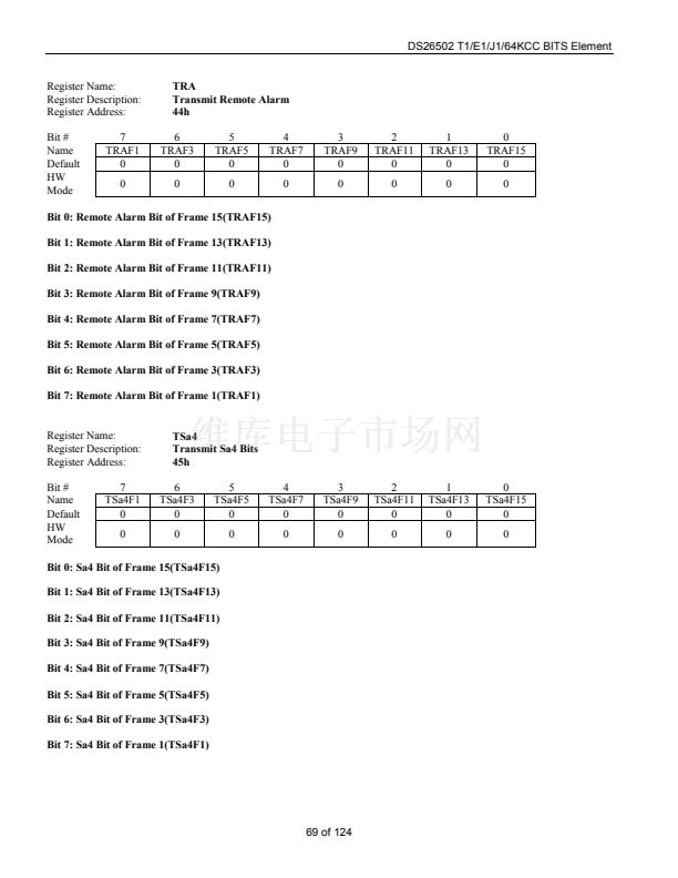
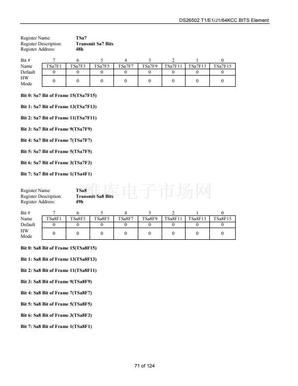
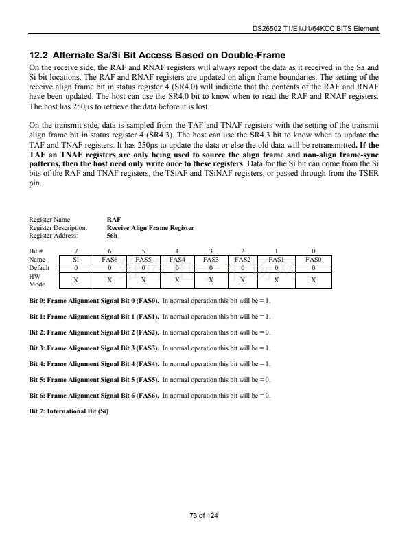
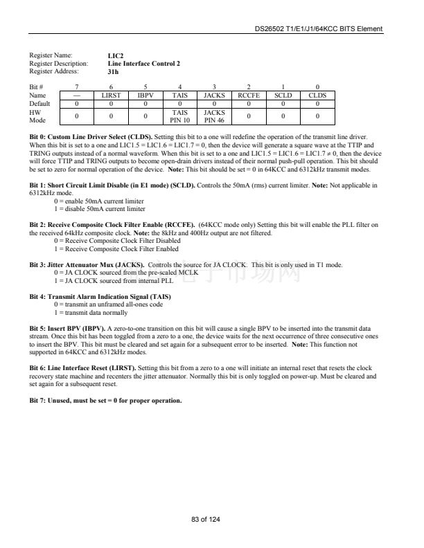
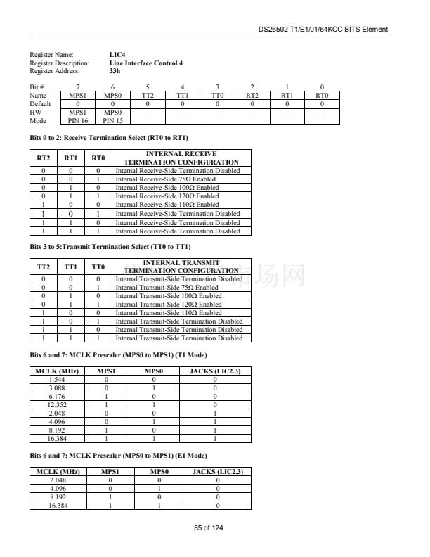
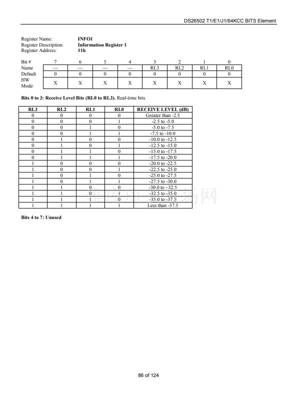
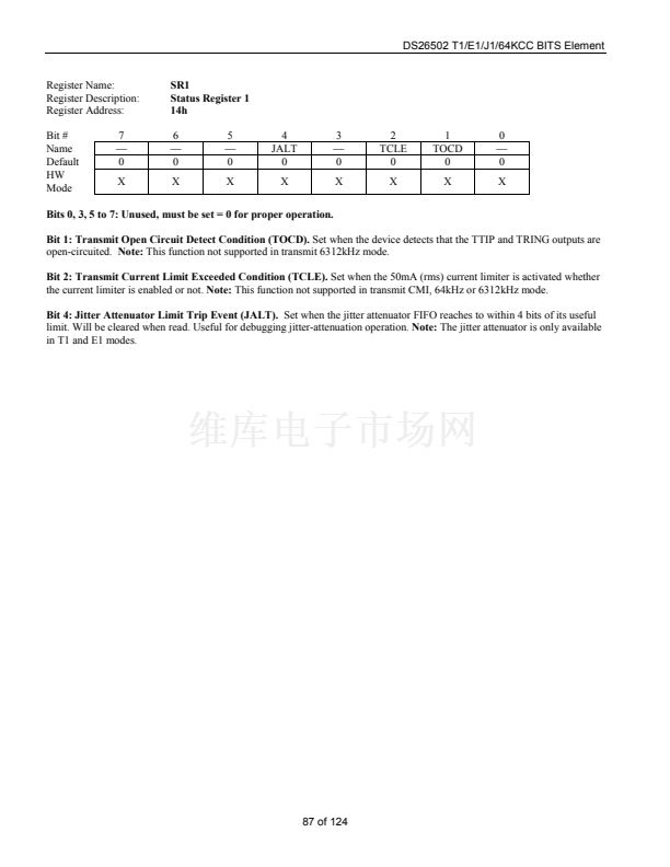
Register Name:
Register Description:
Register Address:
Bit #
Name
Default
HW
Mode
7
L2
0
L2
PIN 13
LIC1
Line Interface Control 1
30h
6
L1
0
L1
PIN 12
5
L0
0
L0
PIN 11
4
EGL
0
0
3
JAS
0
0
2
JABDS
0
0
1
DJA
0
0
0
TPD
0
1
Bit 0: Transmit Power-Down (TPD)
0 = powers down the transmitter and tri-states the TTIP and TRING pins
1 = normal transmitter operation
Bit 1: Disable Jitter Attenuator (DJA). Note:
The jitter attenuator is only available in T1 and E1 modes.
0 = jitter attenuator enabled
1 = jitter attenuator disabled
Bit 2/Jitter Attenuator Buffer Depth Select (JABDS). Note:
The jitter attenuator is only available in T1 and E1 modes.
0 = 128 bits
1 = 32 bits (use for delay-sensitive applications)
Bit 3: Jitter Attenuator Select (JAS). Note:
The jitter attenuator is only available in T1 and E1 modes.
0 = place the jitter attenuator on the receive side
1 = place the jitter attenuator on the transmit side
Bit 4: Receive Equalizer Gain Limit (EGL).
This bit controls the sensitivity of the receive equalizer.
T1 Mode: 0 = -36dB (long haul)
1 = -15dB (limited long haul)
E1 Mode: 0 = -43dB (long haul)
1 = -12dB (short haul)
Bits 5 to 7: Line Build-Out Select (L0 to L2).
When using the internal termination, the user needs only to select 000 for 75鈩?/div>
operation or 001 for 120鈩?operation. This selects the proper voltage levels for 75鈩?or 120鈩?operation. Using TT0 and TT1 of
the LICR4 register, users can then select the proper internal source termination. Line build-outs 100 and 101 are for backwards
compatibility with older products only.
E1 Mode
L2
L1
0
0
0
0
1
0
1
0
L0
0
1
0
1
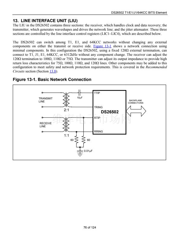
APPLICATION
75鈩?normal
120鈩?normal
75鈩?with high return loss*
120鈩?with high return loss*
N (1)
1:2
1:2
1:2
1:2
RETURN LOSS
N.M.
N.M.
21dB
21dB
Rt (1)
0
0
6.2鈩?/div>
11.6鈩?/div>
*TT0
and TT1 of LIC4 register must be set to zero in this configuration.
81 of 124


 1
1
 2
2
 3
3
 4
4
 5
5
 6
6
 7
7
 8
8
 9
9
 10
10
 11
11
 12
12
 13
13
 14
14
 15
15
 16
16
 17
17
 18
18
 19
19
 20
20
 21
21
 22
22
 23
23
 24
24
 25
25
 26
26
 27
27
 28
28
 29
29
 30
30
 31
31
 32
32
 33
33
 34
34
 35
35
 36
36
 37
37
 38
38
 39
39
 40
40
 41
41
 42
42
 43
43
 44
44
 45
45
 46
46
 47
47
 48
48
 49
49
 50
50
 51
51
 52
52
 53
53
 54
54
 55
55
 56
56
 57
57
 58
58
 59
59
 60
60
 61
61
 62
62
 63
63
 64
64
 65
65
 66
66
 67
67
 68
68
 69
69
 70
70
 71
71
 72
72
 73
73
 74
74
 75
75
 76
76
 77
77
 78
78
 79
79
 80
80
 81
81
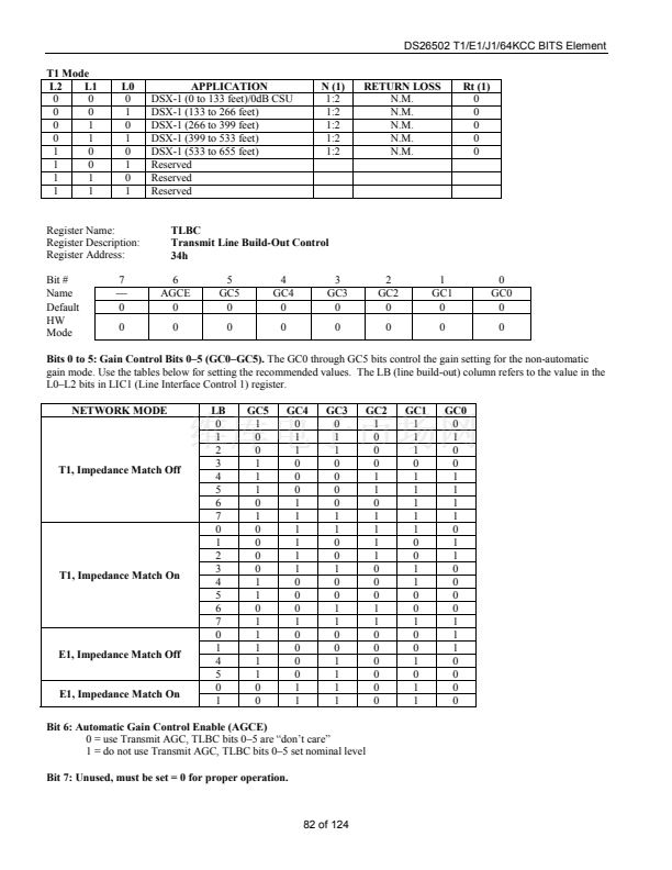 82
82
 83
83
 84
84
 85
85
 86
86
 87
87
 88
88
 89
89
 90
90
 91
91
 92
92
 93
93
 94
94
 95
95
 96
96
 97
97
 98
98
 99
99
 100
100
 101
101
 102
102
 103
103
 104
104
 105
105
 106
106
 107
107
 108
108
 109
109
 110
110
 111
111
 112
112
 113
113
 114
114
 115
115
 116
116
 117
117
 118
118
 119
119
 120
120
 121
121
 122
122
 123
123
 124
124
