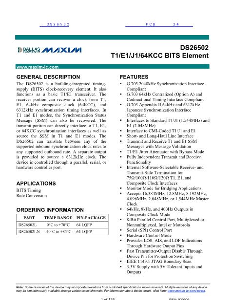
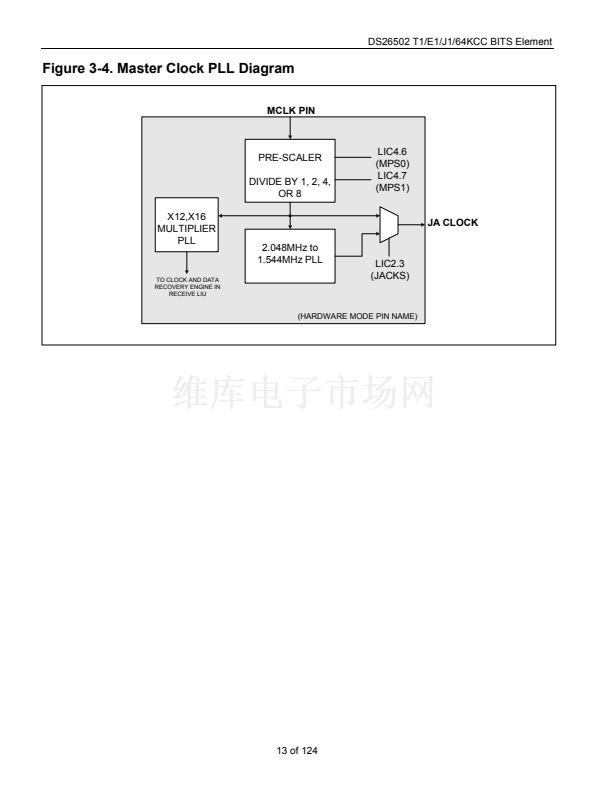
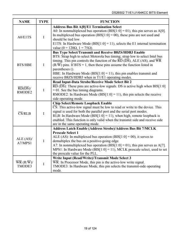
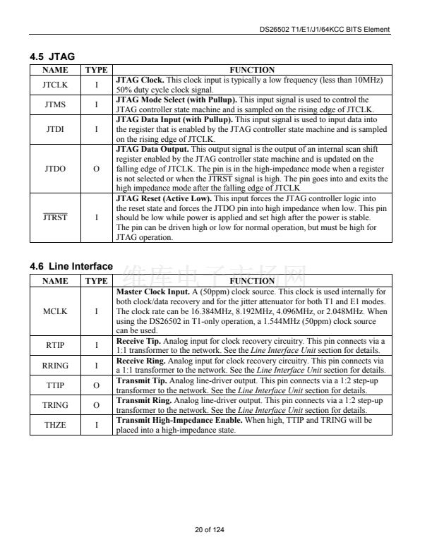
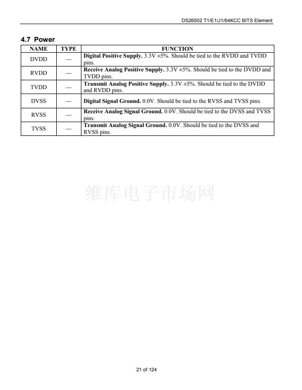
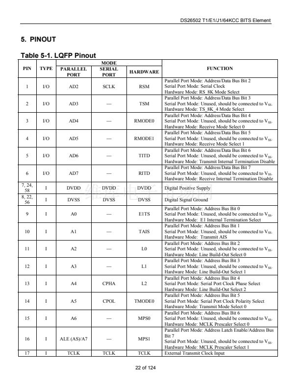
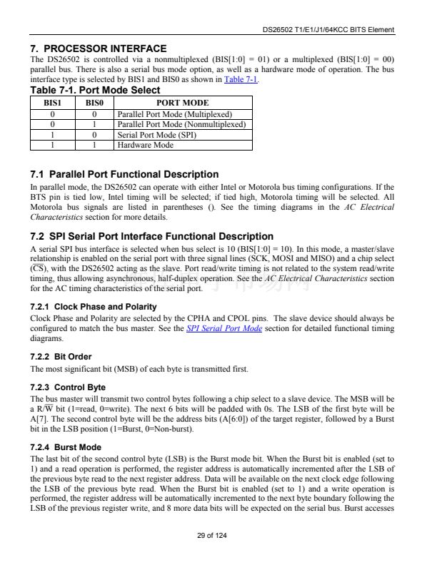
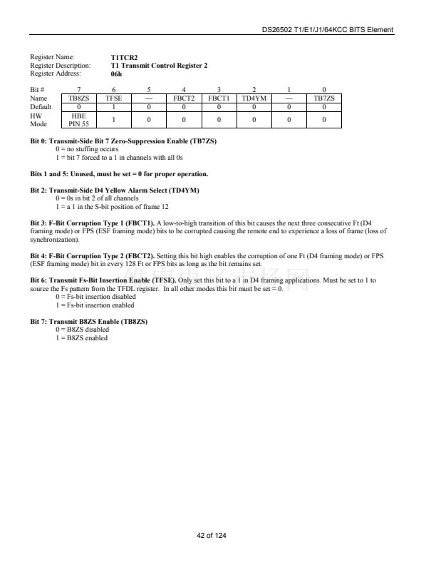
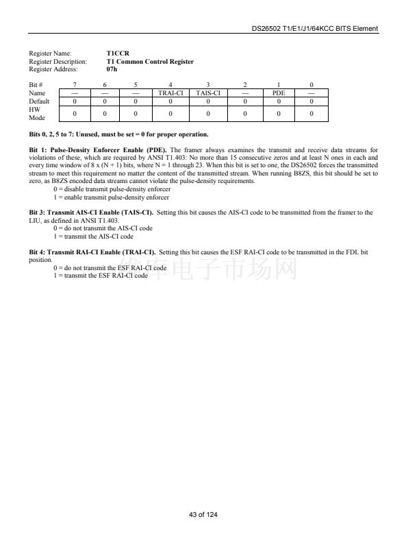
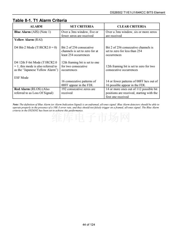
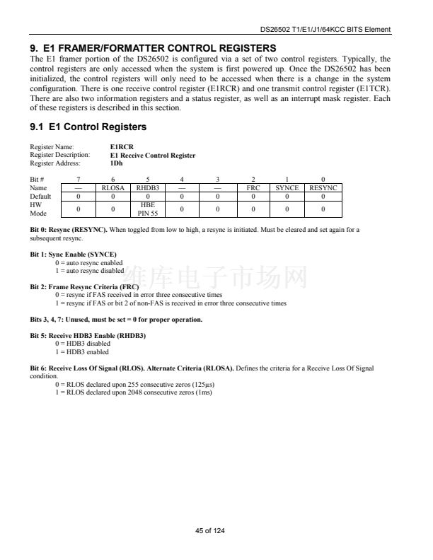
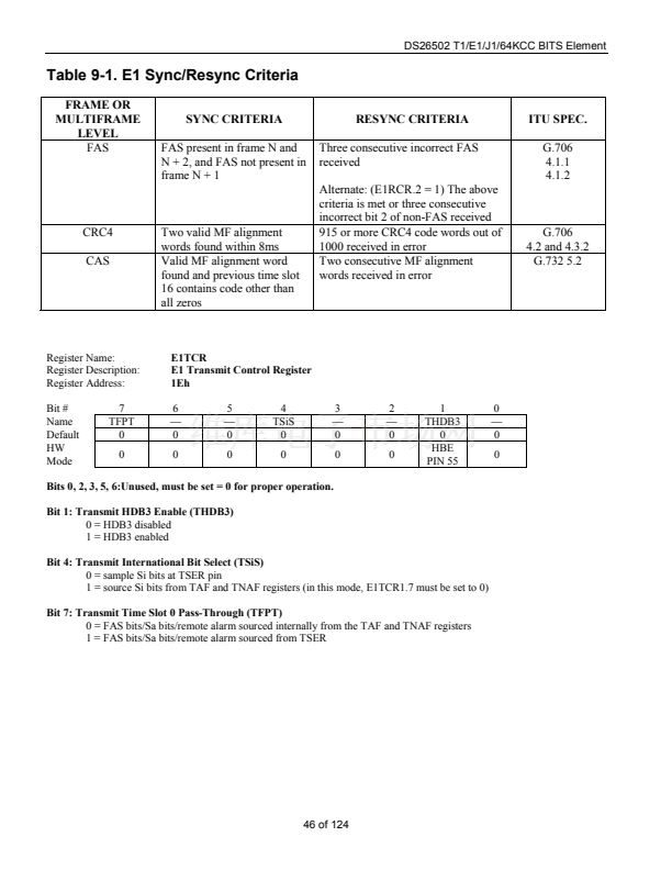
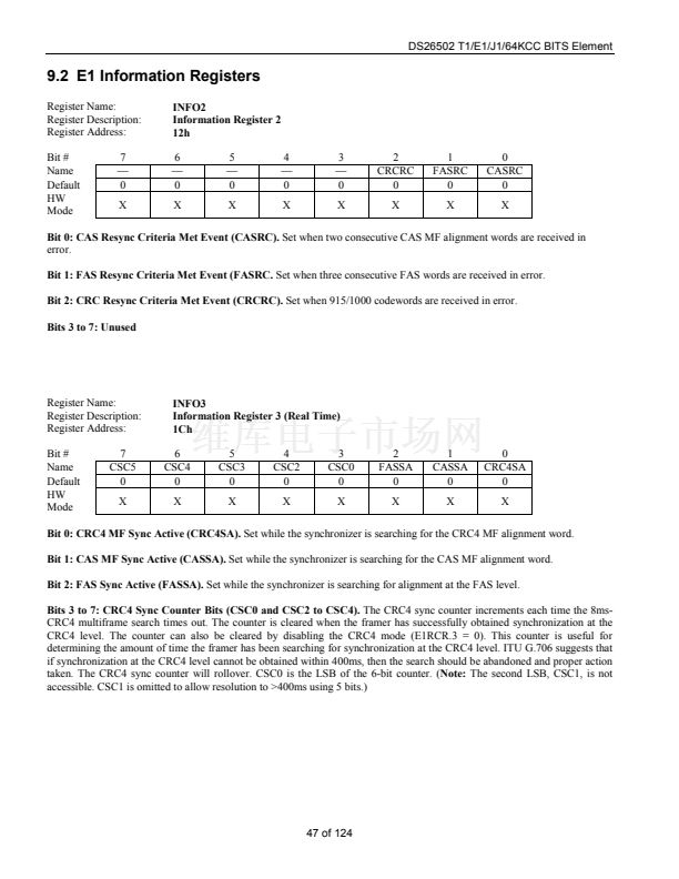
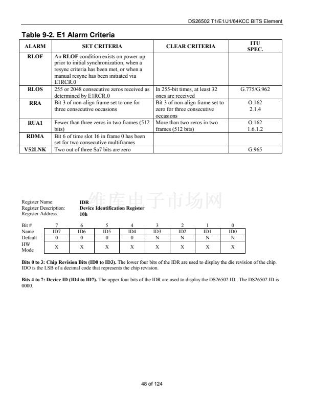
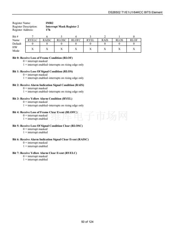
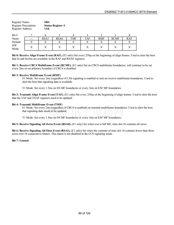
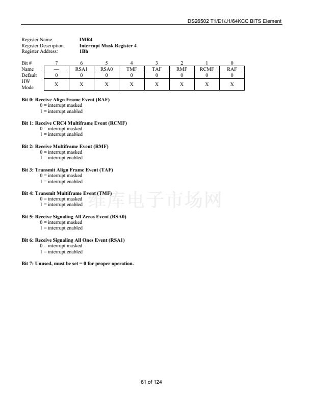
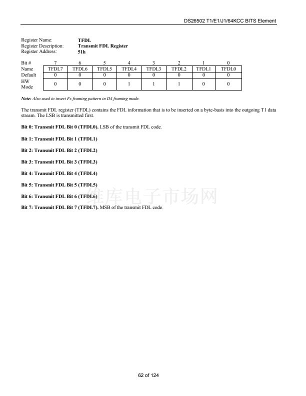
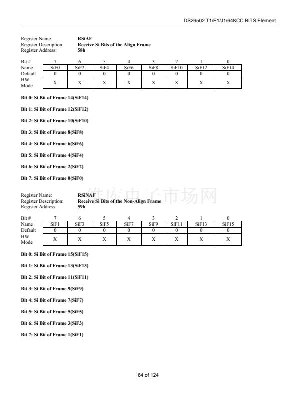
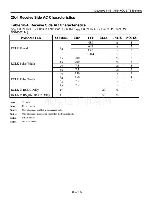
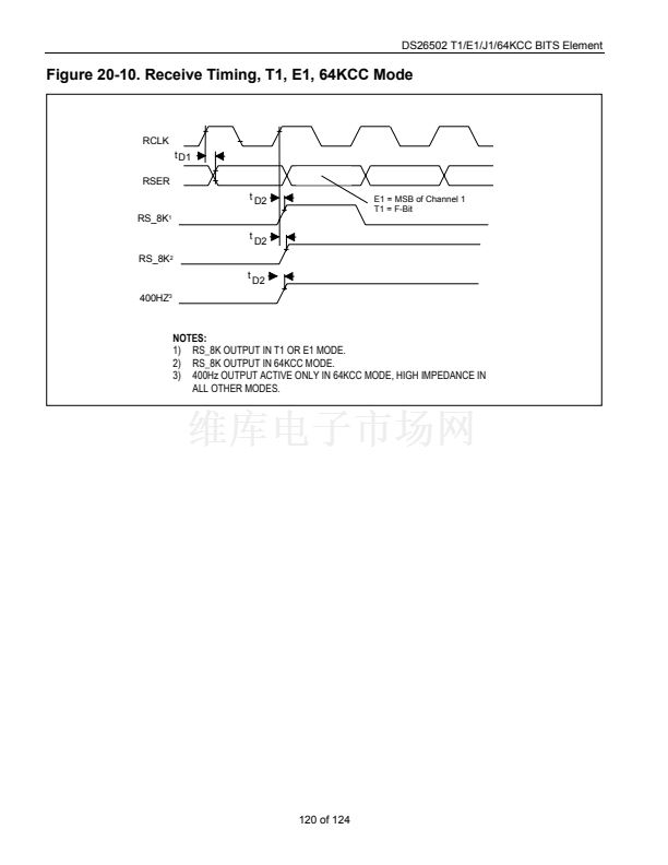
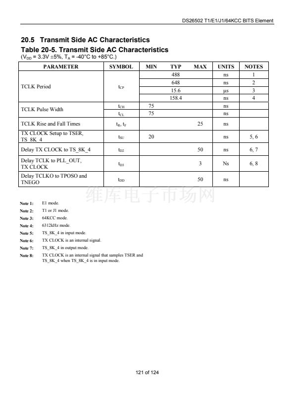
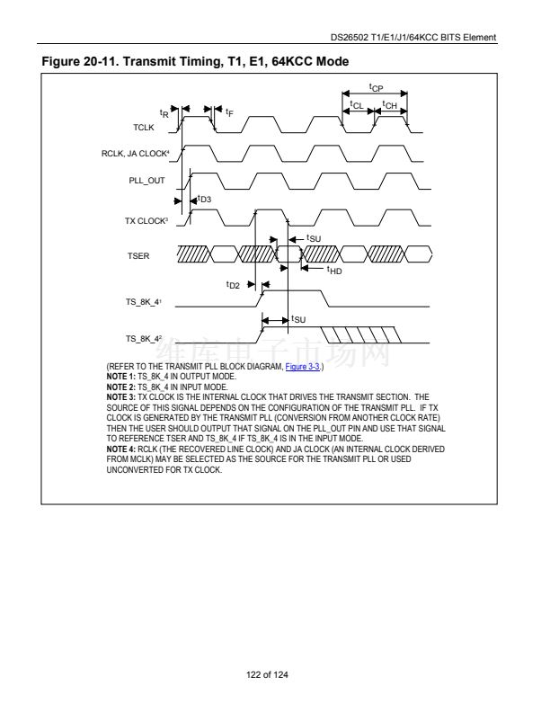
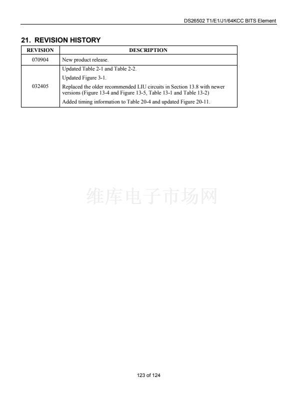
DS26502 T1/E1/J1/64KCC BITS Element
1. FEATURES
1.1 General
搂
搂
搂
搂
搂
搂
搂
搂
搂
搂
搂
搂
搂
搂
搂
搂
搂
搂
搂
搂
搂
搂
搂
搂
搂
搂
搂
搂
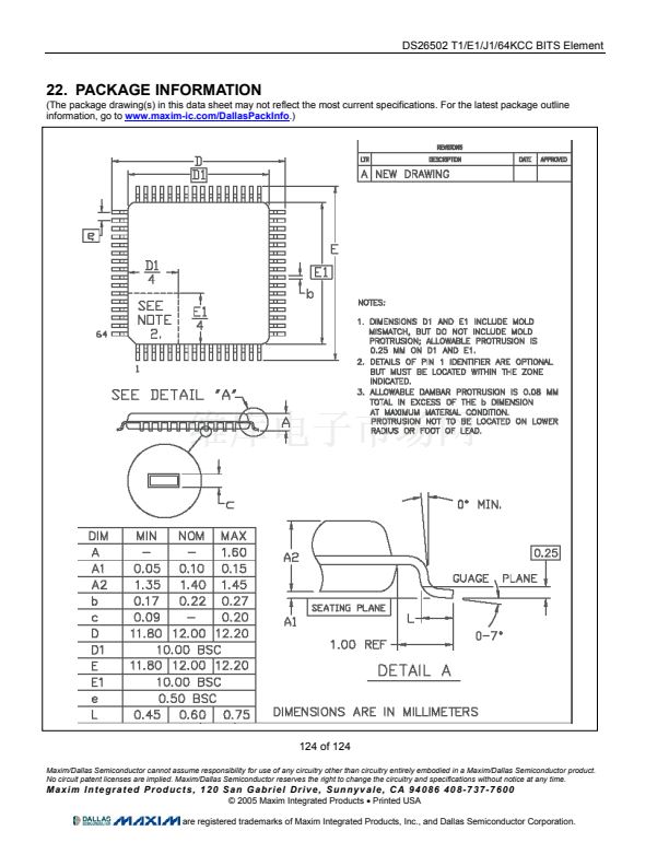
64-pin, 10mm x 10mm LQFP package
3.3V supply with 5V-tolerant inputs and outputs
Evaluation kits
IEEE 1149.1 JTAG Boundary Scan
Driver source code available from the factory
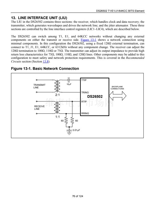
1.2 Line Interface
Requires a single master clock (MCLK) for E1, T1, or J1 operation. Master clock can be
2.048MHz, 4.096MHz, 8.192MHz, or 16.384MHz. Option to use 1.544MHz, 3.088MHz,
6.176MHz, or 12.352MHz for T1-only operation.
Fully software configurable
Short- and long-haul applications
Automatic receive sensitivity adjustments
Ranges include 0dB to -43dB or 0dB to -12dB for E1 applications; 0dB to -36dB or 0dB to -15dB
for T1 applications
Receive level indication in 2.5dB steps from -42.5dB to -2.5dB
Internal receive termination option for 75鈩? 100鈩? 110鈩? and 120鈩?lines
Monitor application gain settings of 20dB, 26dB, and 32dB
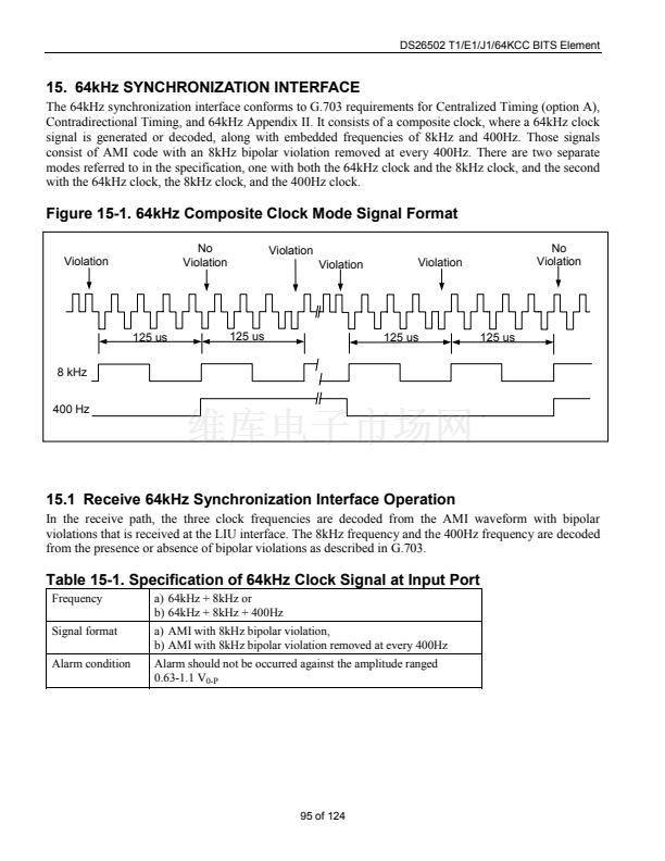
G.703 receive-synchronization signal mode
Flexible transmit-waveform generation
T1 DSX-1 line build-outs
E1 waveforms include G.703 waveshapes for both 75鈩?coax and 120鈩?twisted cables
AIS generation independent of loopbacks
Alternating ones and zeros generation
Square-wave output
Open-drain output option
Transmitter power-down
Transmitter 50mA short-circuit limiter with exceeded indication of current limit
Transmit open-circuit-detected indication
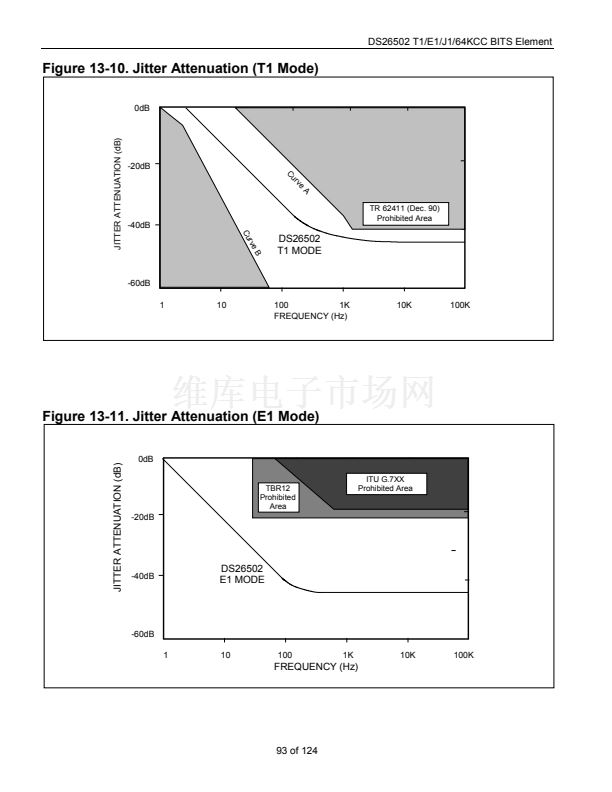
1.3 Jitter Attenuator (T1/E1 Modes Only)
32-bit or 128-bit crystal-less jitter attenuator
Requires only a 2.048MHz master clock for both E1 and T1 operation with the option to use
1.544MHz for T1 operation
Can be placed in either the receive or transmit path or disabled
Limit trip indication
7 of 124


 1
1
 2
2
 3
3
 4
4
 5
5
 6
6
 7
7
 8
8
 9
9
 10
10
 11
11
 12
12
 13
13
 14
14
 15
15
 16
16
 17
17
 18
18
 19
19
 20
20
 21
21
 22
22
 23
23
 24
24
 25
25
 26
26
 27
27
 28
28
 29
29
 30
30
 31
31
 32
32
 33
33
 34
34
 35
35
 36
36
 37
37
 38
38
 39
39
 40
40
 41
41
 42
42
 43
43
 44
44
 45
45
 46
46
 47
47
 48
48
 49
49
 50
50
 51
51
 52
52
 53
53
 54
54
 55
55
 56
56
 57
57
 58
58
 59
59
 60
60
 61
61
 62
62
 63
63
 64
64
 65
65
 66
66
 67
67
 68
68
 69
69
 70
70
 71
71
 72
72
 73
73
 74
74
 75
75
 76
76
 77
77
 78
78
 79
79
 80
80
 81
81
 82
82
 83
83
 84
84
 85
85
 86
86
 87
87
 88
88
 89
89
 90
90
 91
91
 92
92
 93
93
 94
94
 95
95
 96
96
 97
97
 98
98
 99
99
 100
100
 101
101
 102
102
 103
103
 104
104
 105
105
 106
106
 107
107
 108
108
 109
109
 110
110
 111
111
 112
112
 113
113
 114
114
 115
115
 116
116
 117
117
 118
118
 119
119
 120
120
 121
121
 122
122
 123
123
 124
124
