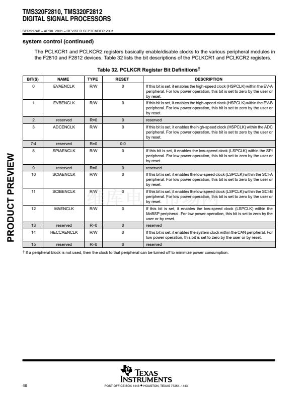
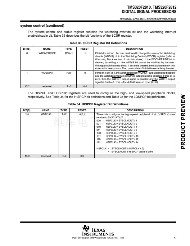
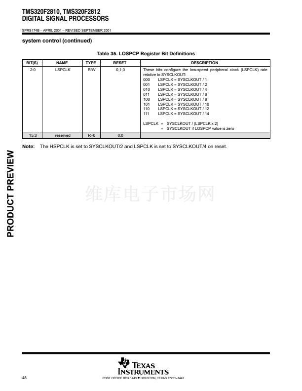
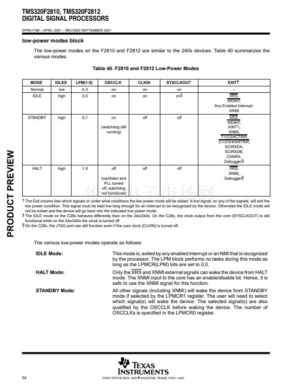
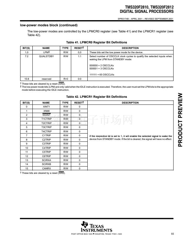
TMS320F2810, TMS320F2812
DIGITAL SIGNAL PROCESSORS
SPRS174B 鈥?APRIL 2001 鈥?REVISED SEPTEMBER 2001
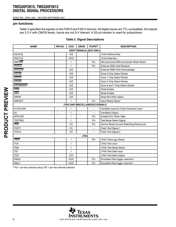
external interface, XINTF (F2812 only) (continued)
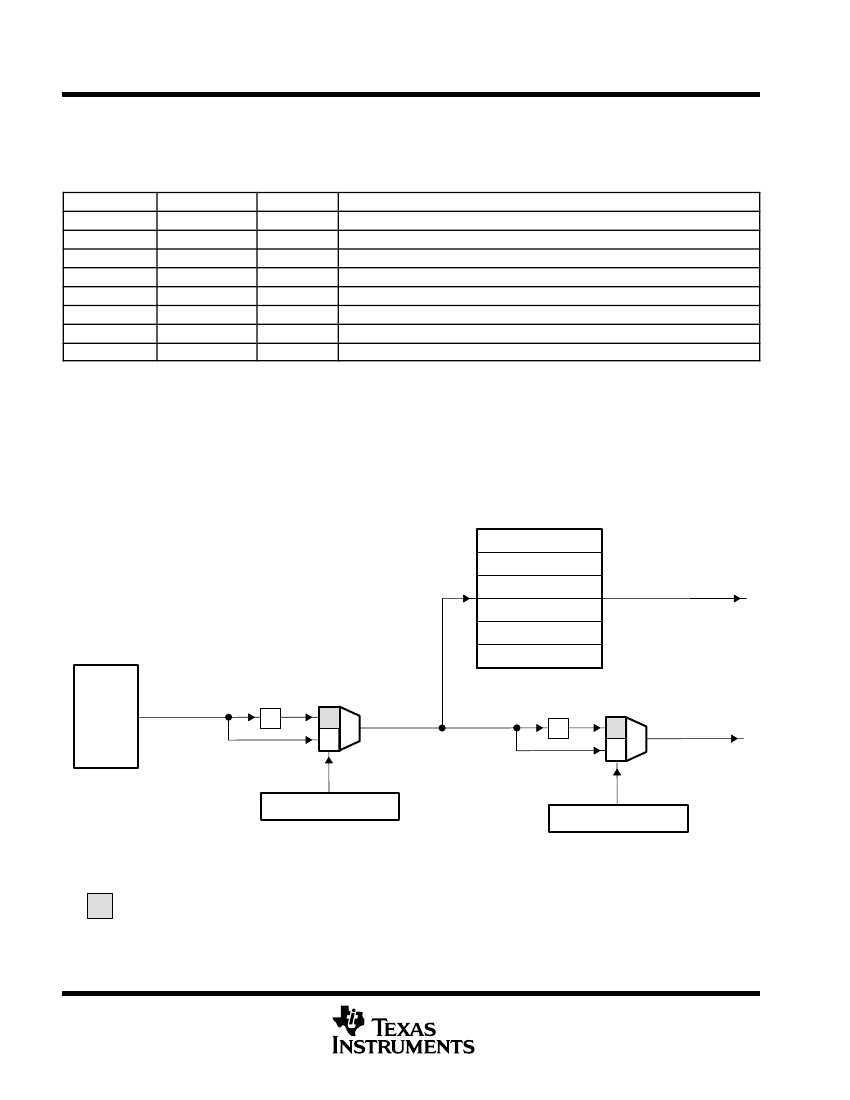
The operation and timing of the external interface, can be controlled by the registers listed in Table 13.
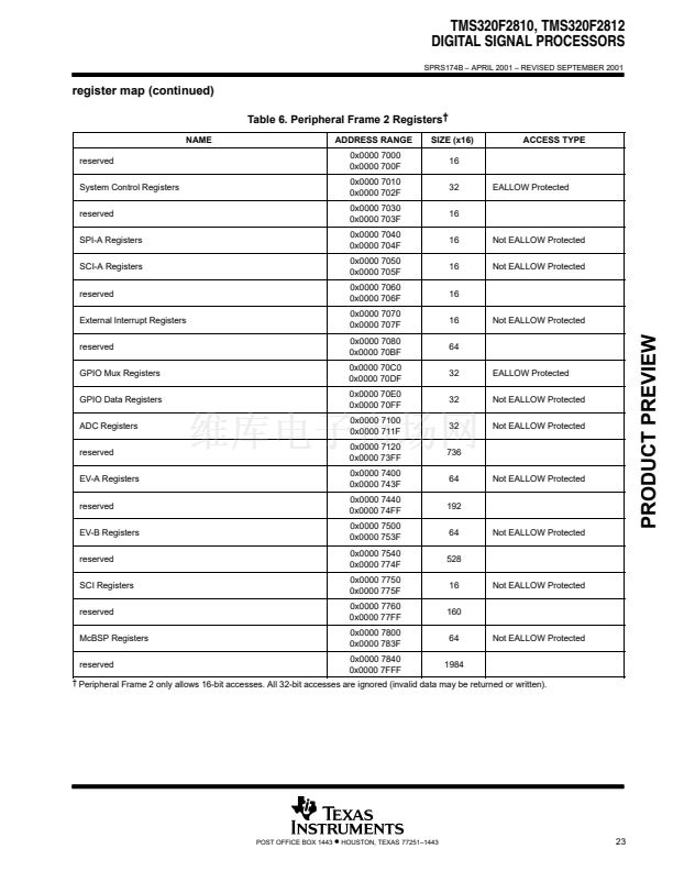
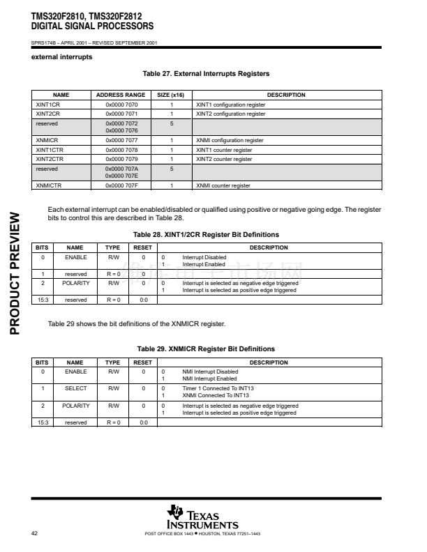
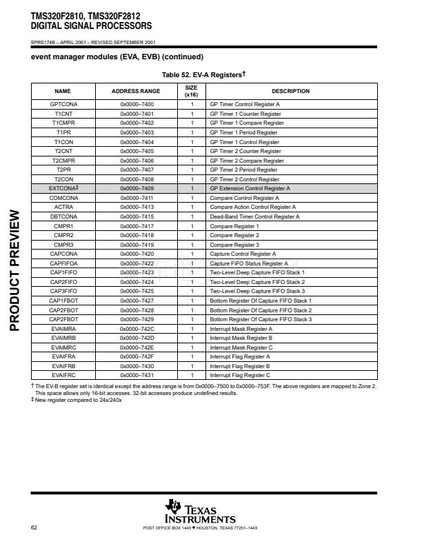
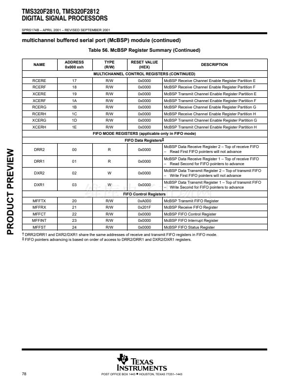
Table 13. XINTF Configuration and Control Register Mappings
NAME
XTIMING0
XTIMING1
XTIMING2
XTIMING6
XTIMING7
XINTCNF2
XBANK
XREVISION
ADDRESS
0x0000鈥?B20
0x0000鈥?B22
0x0000鈥?B24
0x0000鈥?B2C
0x0000鈥?B2E
0x0000鈥?B34
0x0000鈥?B38
0x0000鈥?B3A
SIZE (x16)
2
2
2
2
2
2
1
1
XINTF Timing Register, Zone 0
XINTF Timing Register, Zone 1
XINTF Timing Register, Zone 2
XINTF Timing Register, Zone 6
XINTF Timing Register, Zone 7
XINTF Configuration Register
XINTF Bank Control Register
XINTF Revision Register
DESCRIPTION
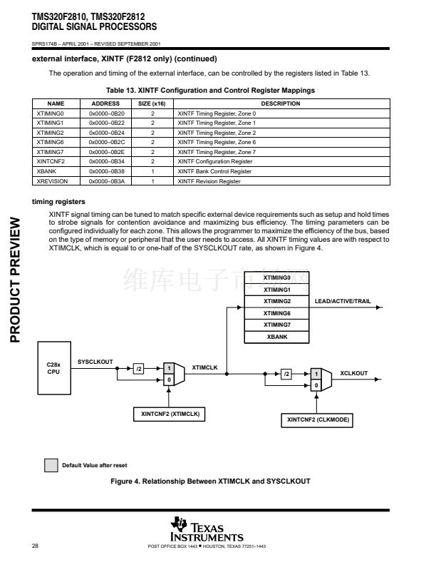
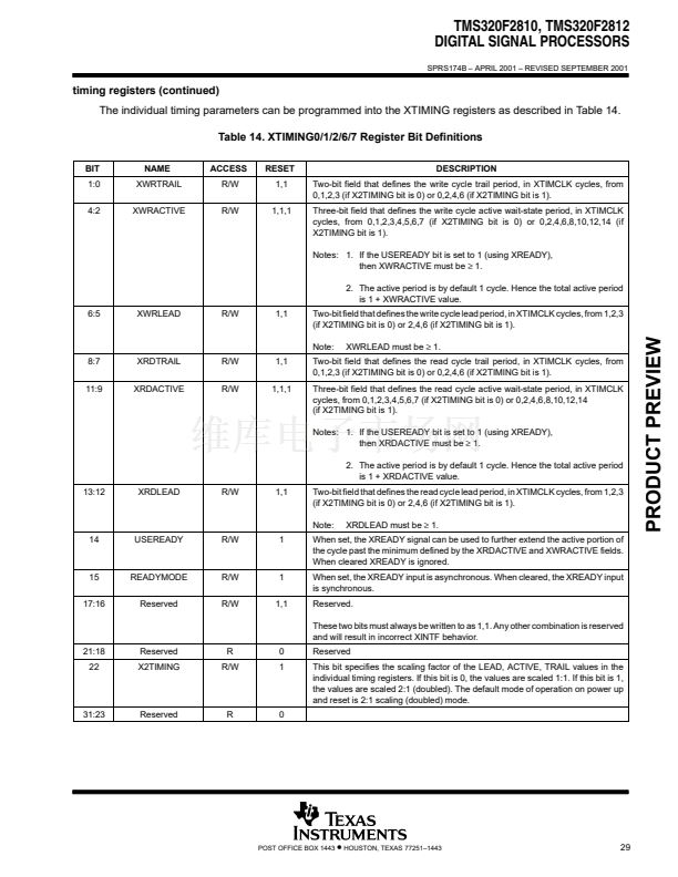
timing registers
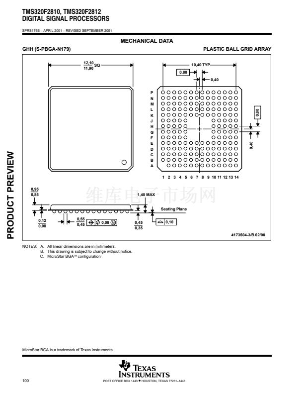
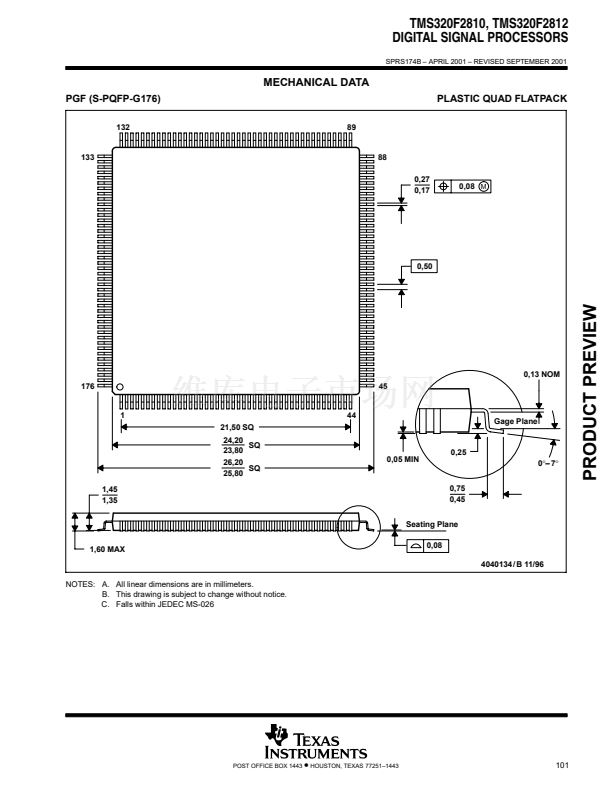
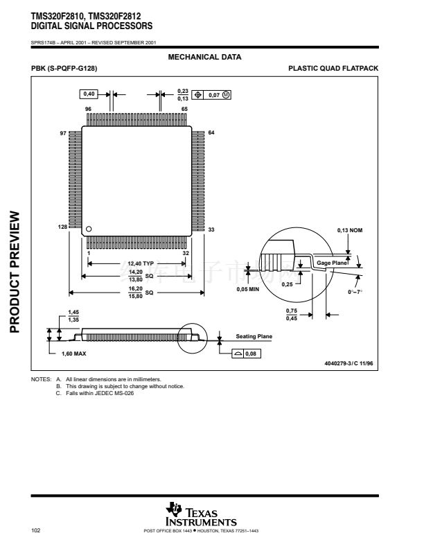
PRODUCT PREVIEW
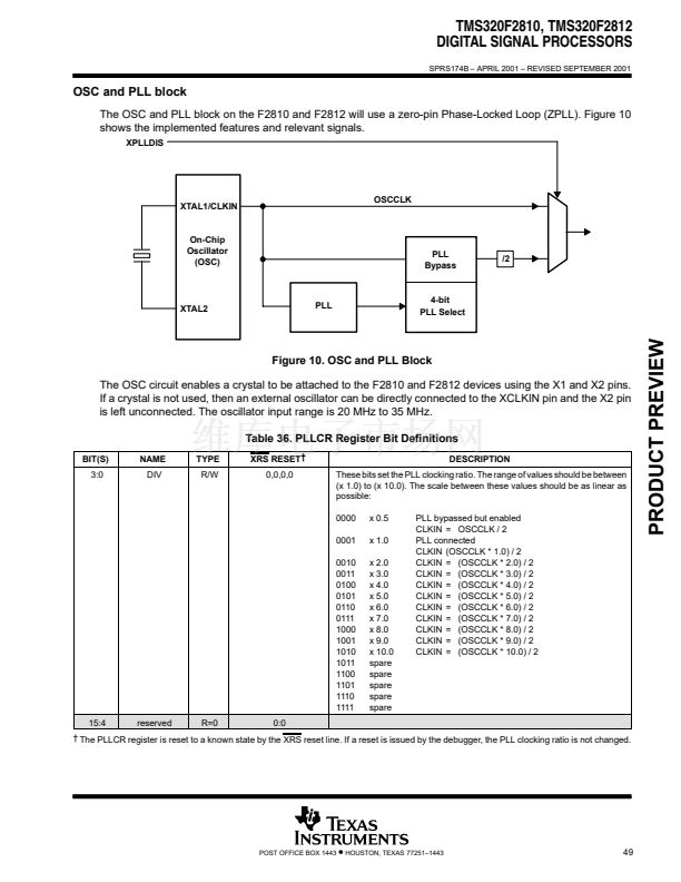
XINTF signal timing can be tuned to match specific external device requirements such as setup and hold times
to strobe signals for contention avoidance and maximizing bus efficiency. The timing parameters can be
configured individually for each zone. This allows the programmer to maximize the efficiency of the bus, based
on the type of memory or peripheral that the user needs to access. All XINTF timing values are with respect to
XTIMCLK, which is equal to or one-half of the SYSCLKOUT rate, as shown in Figure 4.
XTIMING0
XTIMING1
XTIMING2
XTIMING6
XTIMING7
XBANK
LEAD/ACTIVE/TRAIL
C28x
CPU
SYSCLKOUT
/2
1
0
0
XTIMCLK
/2
1
XCLKOUT
XINTCNF2 (XTIMCLK)
XINTCNF2 (CLKMODE)
Default Value after reset
Figure 4. Relationship Between XTIMCLK and SYSCLKOUT
28
POST OFFICE BOX 1443
鈥?/div>
HOUSTON, TEXAS 77251鈥?443


 1
1
 2
2
 3
3
 4
4
 5
5
 6
6
 7
7
 8
8
 9
9
 10
10
 11
11
 12
12
 13
13
 14
14
 15
15
 16
16
 17
17
 18
18
 19
19
 20
20
 21
21
 22
22
 23
23
 24
24
 25
25
 26
26
 27
27
 28
28
 29
29
 30
30
 31
31
 32
32
 33
33
 34
34
 35
35
 36
36
 37
37
 38
38
 39
39
 40
40
 41
41
 42
42
 43
43
 44
44
 45
45
 46
46
 47
47
 48
48
 49
49
 50
50
 51
51
 52
52
 53
53
 54
54
 55
55
 56
56
 57
57
 58
58
 59
59
 60
60
 61
61
 62
62
 63
63
 64
64
 65
65
 66
66
 67
67
 68
68
 69
69
 70
70
 71
71
 72
72
 73
73
 74
74
 75
75
 76
76
 77
77
 78
78
 79
79
 80
80
 81
81
 82
82
 83
83
 84
84
 85
85
 86
86
 87
87
 88
88
 89
89
 90
90
 91
91
 92
92
 93
93
 94
94
 95
95
 96
96
 97
97
 98
98
 99
99
 100
100
 101
101
 102
102
 103
103
