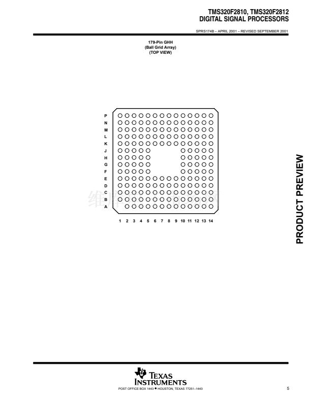
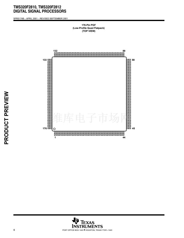
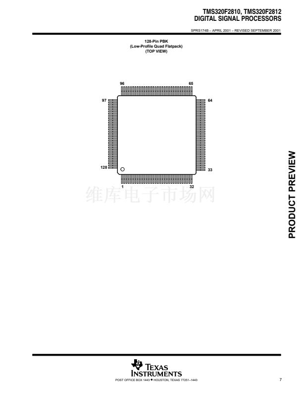
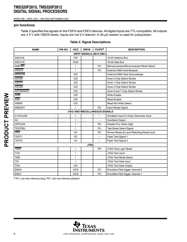
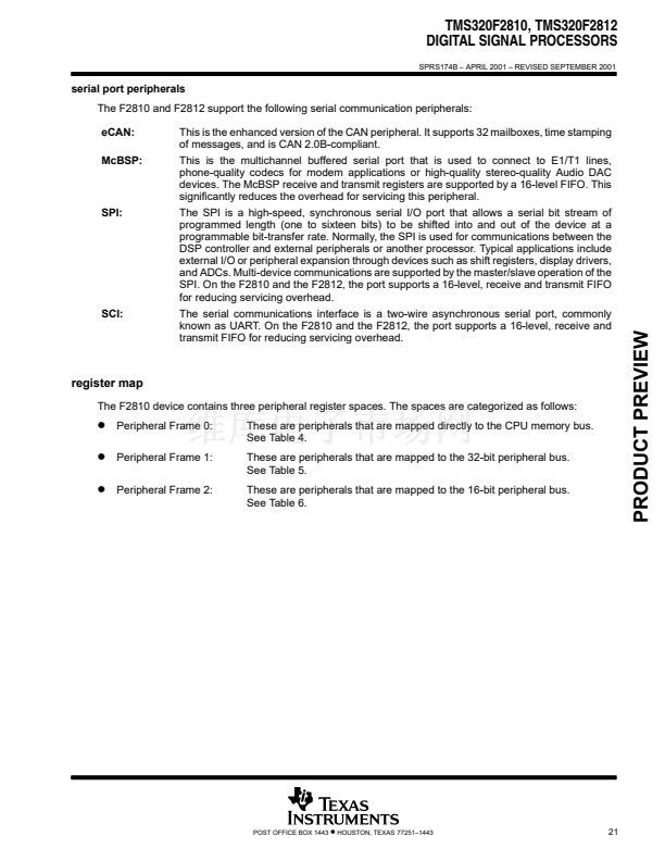
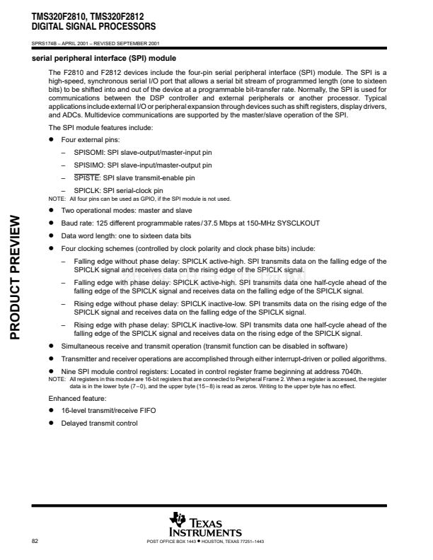
TMS320F2810, TMS320F2812
DIGITAL SIGNAL PROCESSORS
SPRS174B 鈥?APRIL 2001 鈥?REVISED SEPTEMBER 2001
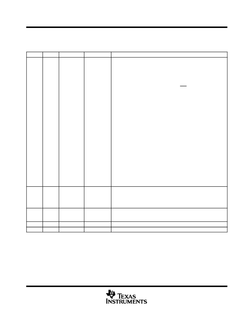
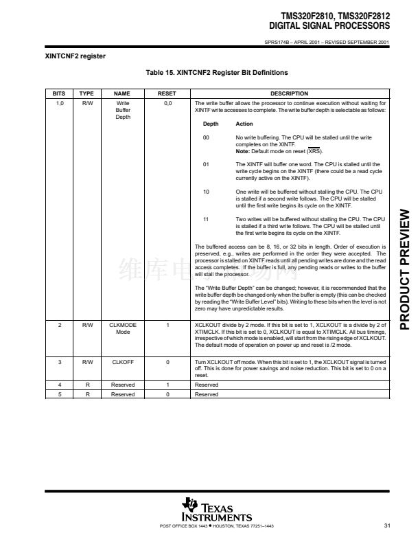
XINTCNF2 register
Table 15. XINTCNF2 Register Bit Definitions
BITS
1,0
TYPE
R/W
NAME
Write
Buffer
Depth
RESET
0,0
DESCRIPTION
The write buffer allows the processor to continue execution without waiting for
XINTF write accesses to complete. The write buffer depth is selectable as follows:
Depth
00
Action
No write buffering. The CPU will be stalled until the write
completes on the XINTF.
Note:
Default mode on reset (XRS).
The XINTF will buffer one word. The CPU is stalled until the
write cycle begins on the XINTF (there could be a read cycle
currently active on the XINTF).
One write will be buffered without stalling the CPU. The CPU
is stalled if a second write follows. The CPU will be stalled
until the first write begins its cycle on the XINTF.
Two writes will be buffered without stalling the CPU. The CPU
is stalled if a third write follows. The CPU will be stalled until
the first write begins its cycle on the XINTF.
01
10
11
The buffered access can be 8, 16, or 32 bits in length. Order of execution is
preserved, e.g., writes are performed in the order they were accepted. The
processor is stalled on XINTF reads until all pending writes are done and the read
access completes. If the buffer is full, any pending reads or writes to the buffer
will stall the processor.
The 鈥淲rite Buffer Depth鈥?can be changed; however, it is recommended that the
write buffer depth be changed only when the buffer is empty (this can be checked
by reading the 鈥淲rite Buffer Level鈥?bits). Writing to these bits when the level is not
zero may have unpredictable results.
2
R/W
CLKMODE
Mode
1
XCLKOUT divide by 2 mode. If this bit is set to 1, XCLKOUT is a divide by 2 of
XTIMCLK. If this bit is set to 0, XCLKOUT is equal to XTIMCLK. All bus timings,
irrespective of which mode is enabled, will start from the rising edge of XCLKOUT.
The default mode of operation on power up and reset is /2 mode.
Turn XCLKOUT off mode. When this bit is set to 1, the XCLKOUT signal is turned
off. This is done for power savings and noise reduction. This bit is set to 0 on a
reset.
Reserved
Reserved
3
R/W
CLKOFF
0
4
5
R
R
Reserved
Reserved
1
0
POST OFFICE BOX 1443
鈥?/div>
HOUSTON, TEXAS 77251鈥?443
31
PRODUCT PREVIEW


 1
1
 2
2
 3
3
 4
4
 5
5
 6
6
 7
7
 8
8
 9
9
 10
10
 11
11
 12
12
 13
13
 14
14
 15
15
 16
16
 17
17
 18
18
 19
19
 20
20
 21
21
 22
22
 23
23
 24
24
 25
25
 26
26
 27
27
 28
28
 29
29
 30
30
 31
31
 32
32
 33
33
 34
34
 35
35
 36
36
 37
37
 38
38
 39
39
 40
40
 41
41
 42
42
 43
43
 44
44
 45
45
 46
46
 47
47
 48
48
 49
49
 50
50
 51
51
 52
52
 53
53
 54
54
 55
55
 56
56
 57
57
 58
58
 59
59
 60
60
 61
61
 62
62
 63
63
 64
64
 65
65
 66
66
 67
67
 68
68
 69
69
 70
70
 71
71
 72
72
 73
73
 74
74
 75
75
 76
76
 77
77
 78
78
 79
79
 80
80
 81
81
 82
82
 83
83
 84
84
 85
85
 86
86
 87
87
 88
88
 89
89
 90
90
 91
91
 92
92
 93
93
 94
94
 95
95
 96
96
 97
97
 98
98
 99
99
 100
100
 101
101
 102
102
 103
103
