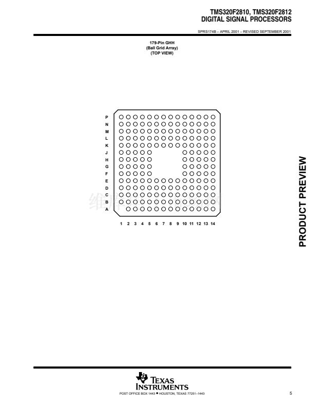
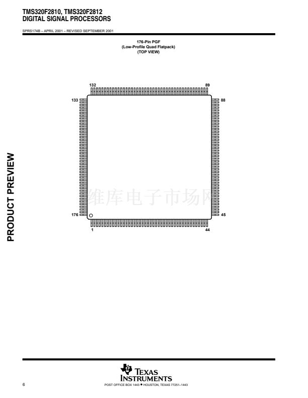
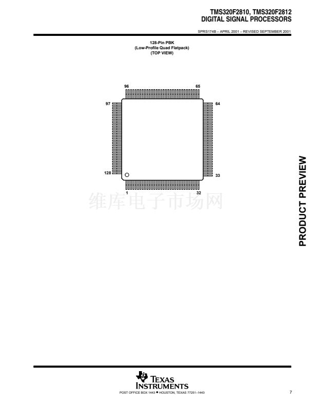
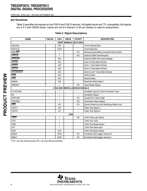
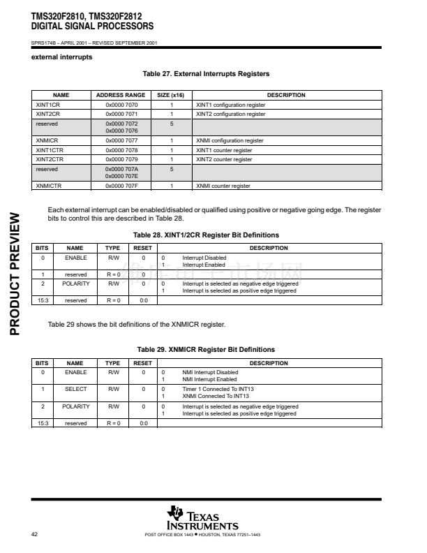
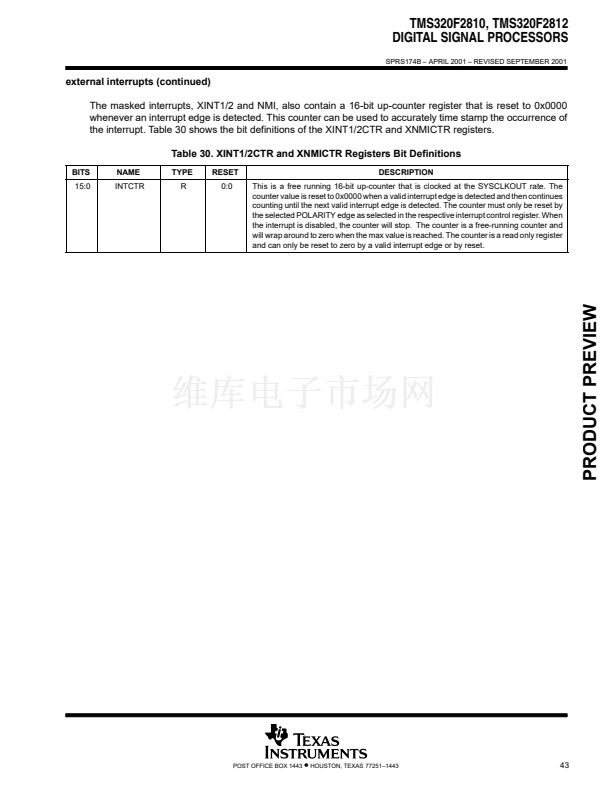
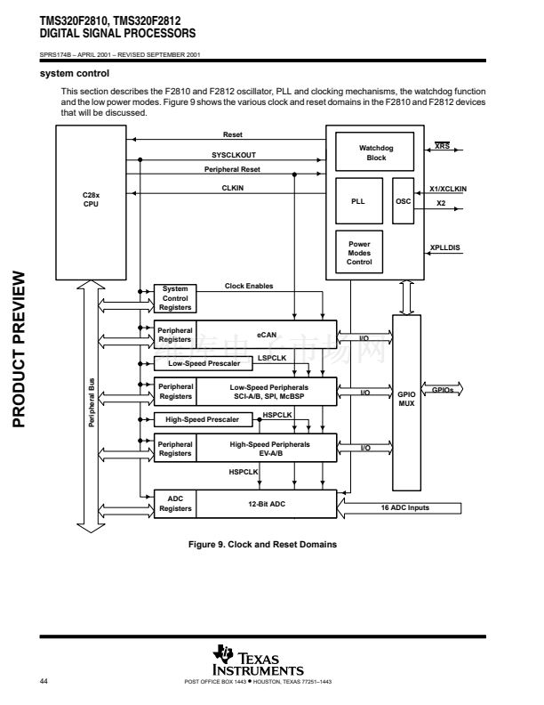
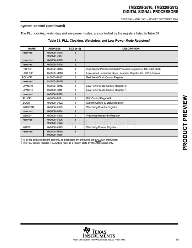
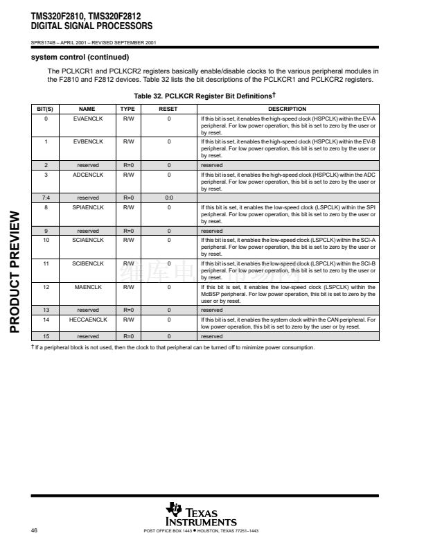
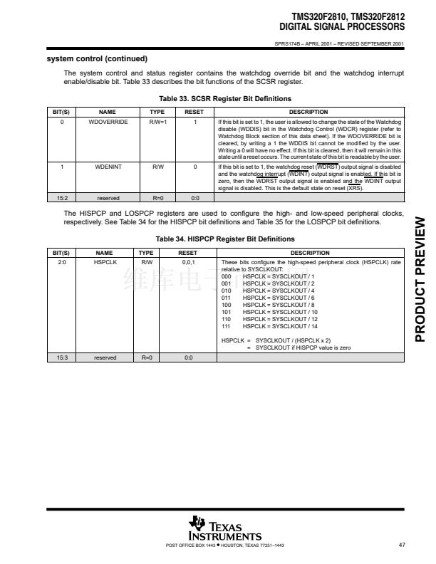
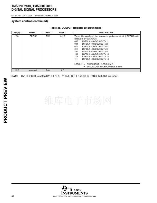
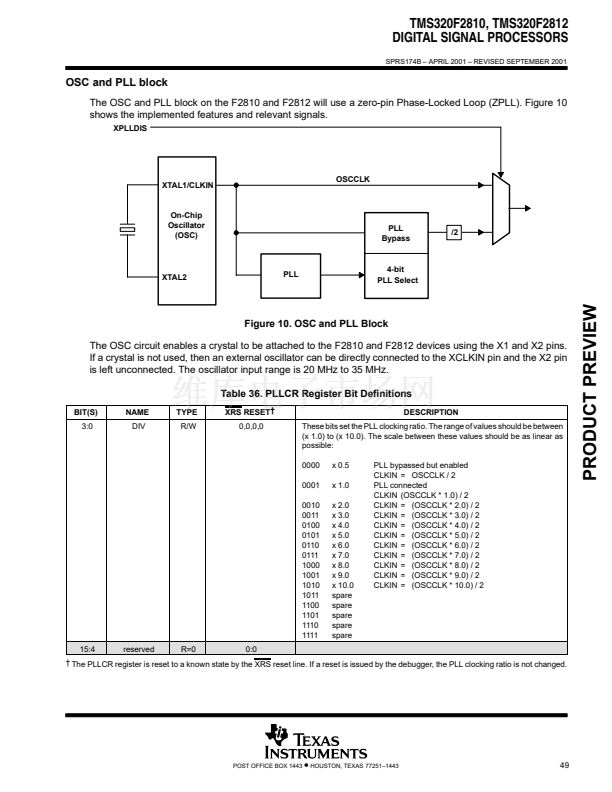
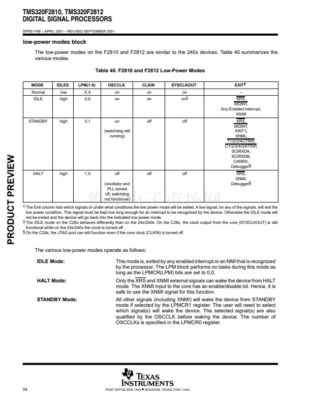
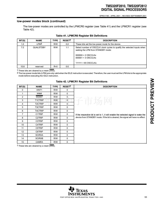
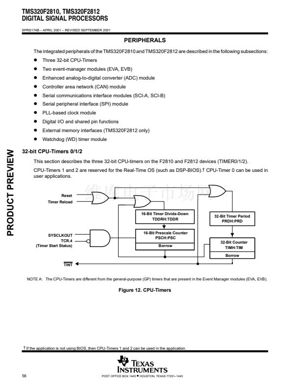
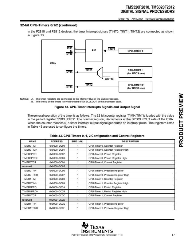
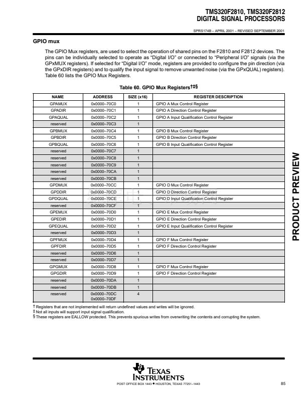
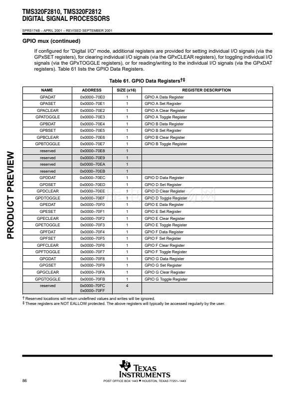
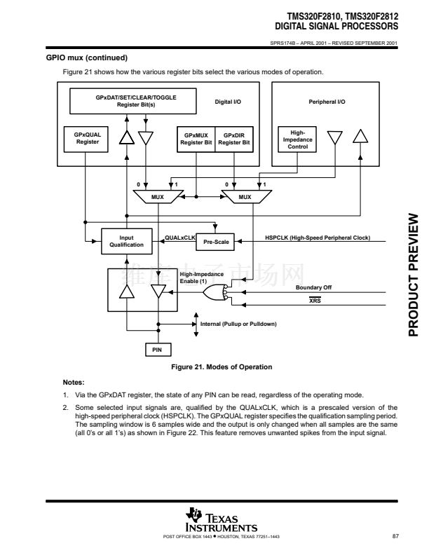
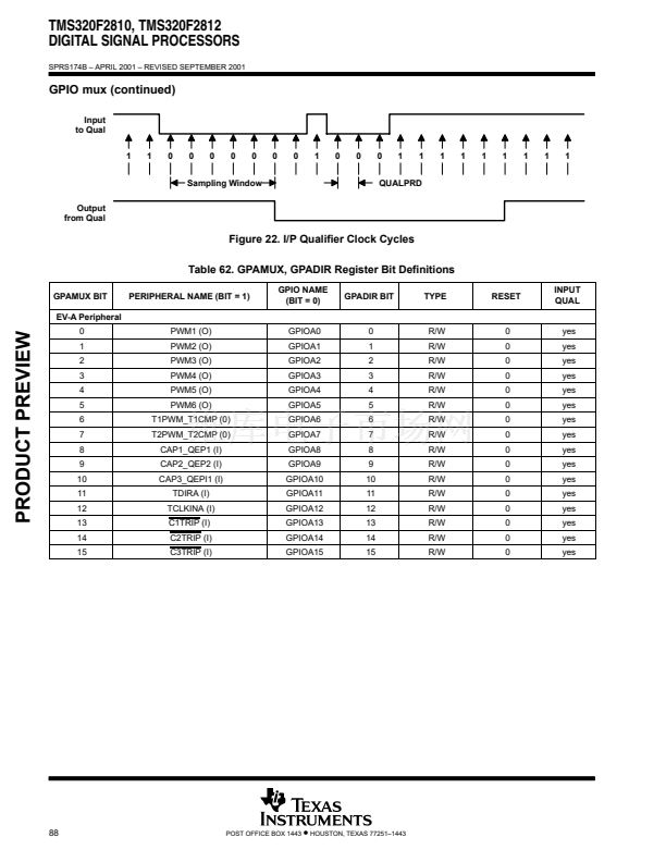
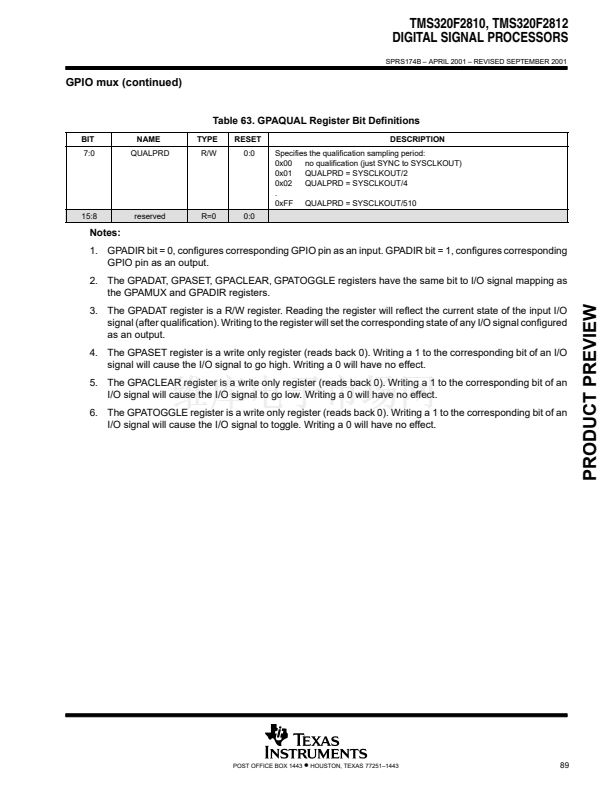
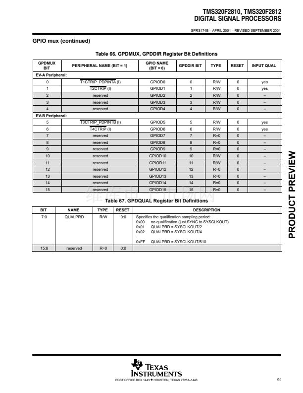
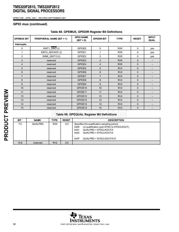
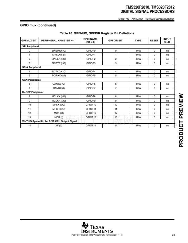
TMS320F2810, TMS320F2812
DIGITAL SIGNAL PROCESSORS
SPRS174B 鈥?APRIL 2001 鈥?REVISED SEPTEMBER 2001
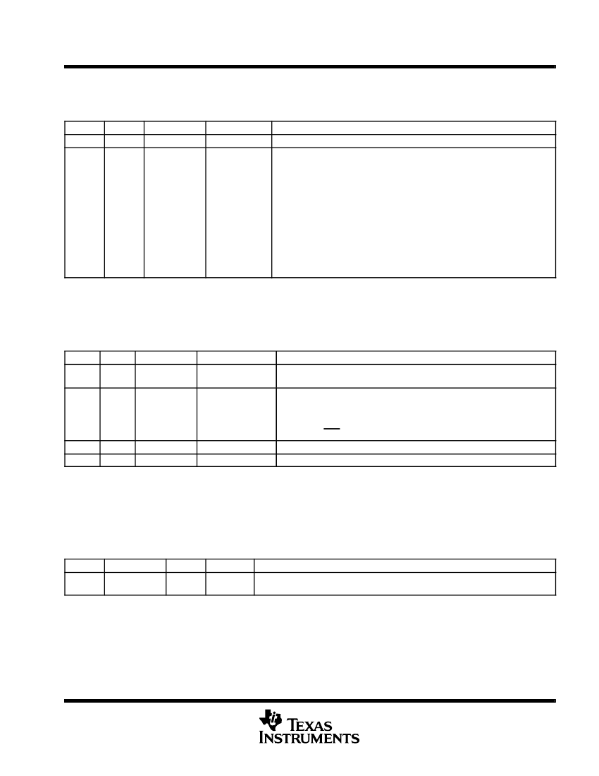
XINTCNF2 register (continued)
Table 15. XINTCNF2 Register Bit Definitions (Continued)
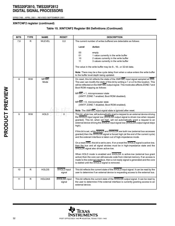
BITS
15:12
18:16
TYPE
X
R/W
NAME
Reserved
XTIMCLK
RESET
0
0,0,1
Reserved
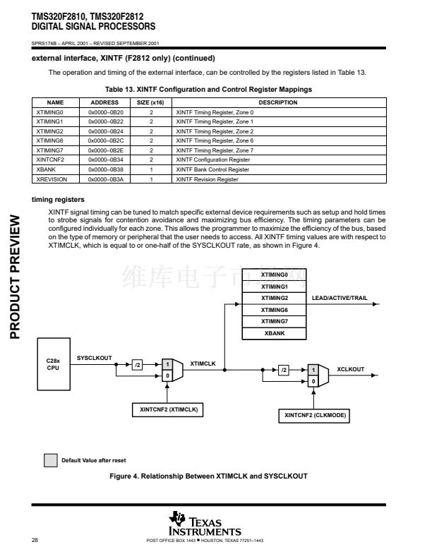
These bits select the fundamental clock for the timing of lead, active and trail
switching operations as defined by the XTIMING and XBANK registers:
Mode
0,0,0
0,0,1
0,1,0
0,1,1
1,0,0
1,0,1
1,1,0
1,1,1
Action
XTIMCLK = SYSCLKOUT/1
XTIMCLK = SYSCLKOUT/2
reserved
reserved
reserved
reserved
reserved
reserved
DESCRIPTION
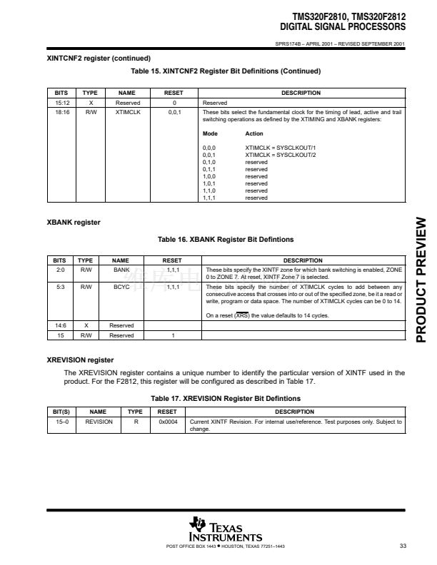
XBANK register
Table 16. XBANK Register Bit Defintions
BITS
2:0
5:3
TYPE
R/W
R/W
NAME
BANK
BCYC
RESET
1,1,1
1,1,1
DESCRIPTION
These bits specify the XINTF zone for which bank switching is enabled, ZONE
0 to ZONE 7. At reset, XINTF Zone 7 is selected.
These bits specify the number of XTIMCLK cycles to add between any
consecutive access that crosses into or out of the specified zone, be it a read or
write, program or data space. The number of XTIMCLK cycles can be 0 to 14.
On a reset (XRS) the value defaults to 14 cycles.
14:6
15
X
R/W
Reserved
Reserved
1
XREVISION register
The XREVISION register contains a unique number to identify the particular version of XINTF used in the
product. For the F2812, this register will be configured as described in Table 17.
Table 17. XREVISION Register Bit Defintions
BIT(S)
15鈥?
NAME
REVISION
TYPE
R
RESET
0x0004
DESCRIPTION
Current XINTF Revision. For internal use/reference. Test purposes only. Subject to
change.
POST OFFICE BOX 1443
鈥?/div>
HOUSTON, TEXAS 77251鈥?443
33
PRODUCT PREVIEW


 1
1
 2
2
 3
3
 4
4
 5
5
 6
6
 7
7
 8
8
 9
9
 10
10
 11
11
 12
12
 13
13
 14
14
 15
15
 16
16
 17
17
 18
18
 19
19
 20
20
 21
21
 22
22
 23
23
 24
24
 25
25
 26
26
 27
27
 28
28
 29
29
 30
30
 31
31
 32
32
 33
33
 34
34
 35
35
 36
36
 37
37
 38
38
 39
39
 40
40
 41
41
 42
42
 43
43
 44
44
 45
45
 46
46
 47
47
 48
48
 49
49
 50
50
 51
51
 52
52
 53
53
 54
54
 55
55
 56
56
 57
57
 58
58
 59
59
 60
60
 61
61
 62
62
 63
63
 64
64
 65
65
 66
66
 67
67
 68
68
 69
69
 70
70
 71
71
 72
72
 73
73
 74
74
 75
75
 76
76
 77
77
 78
78
 79
79
 80
80
 81
81
 82
82
 83
83
 84
84
 85
85
 86
86
 87
87
 88
88
 89
89
 90
90
 91
91
 92
92
 93
93
 94
94
 95
95
 96
96
 97
97
 98
98
 99
99
 100
100
 101
101
 102
102
 103
103
