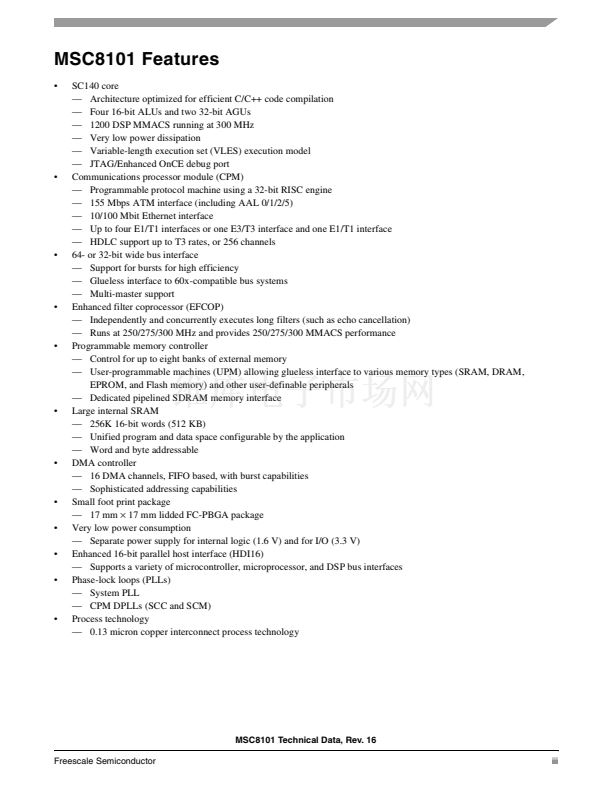
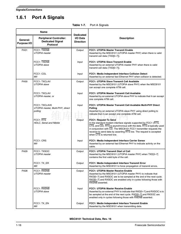
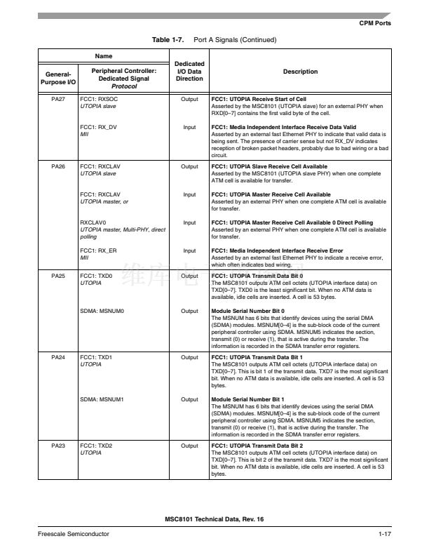
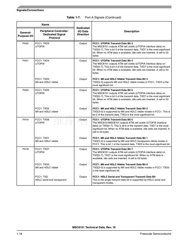
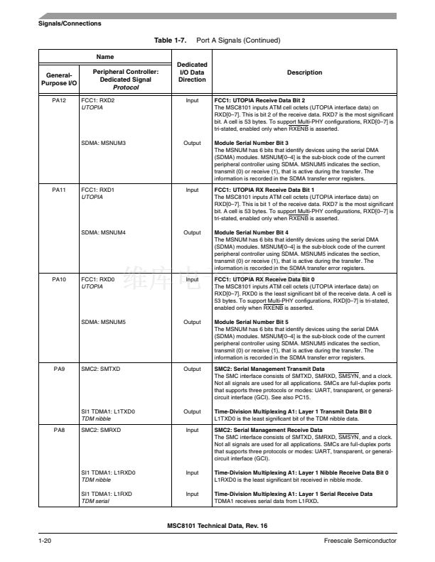
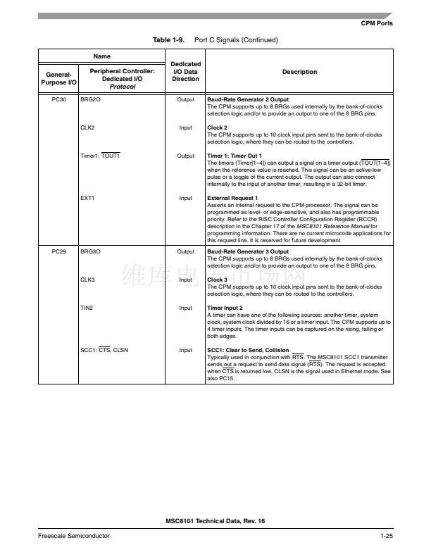
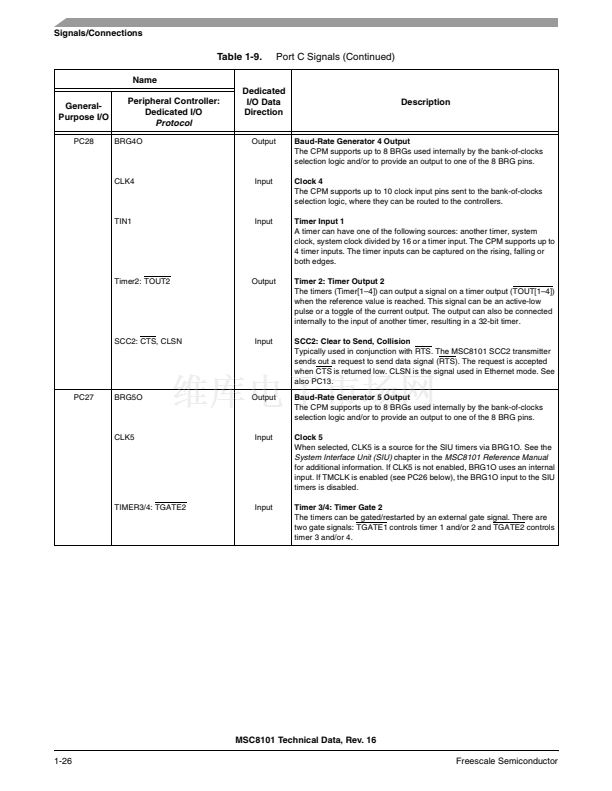
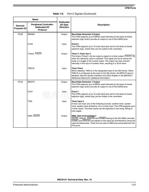
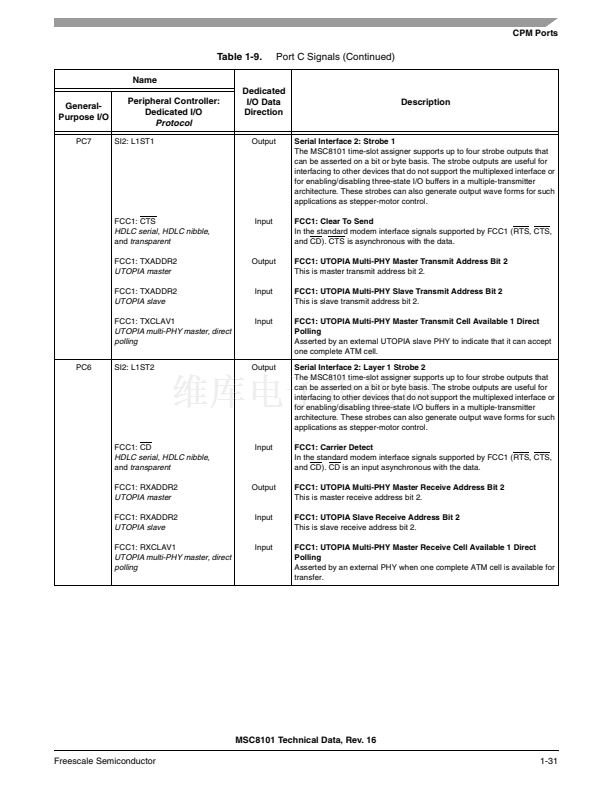
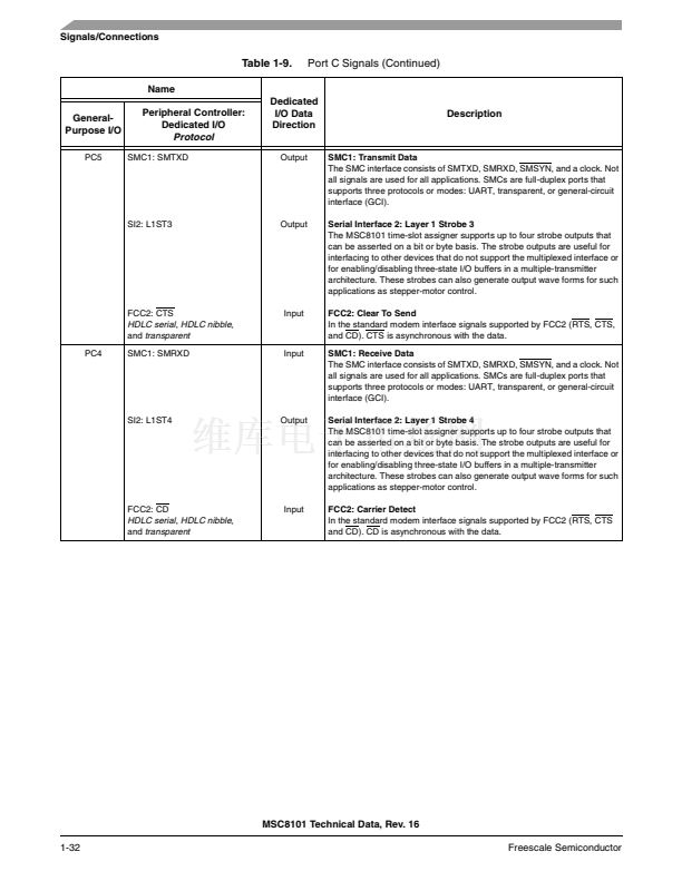
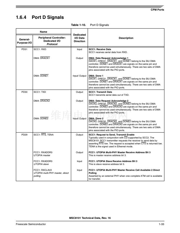
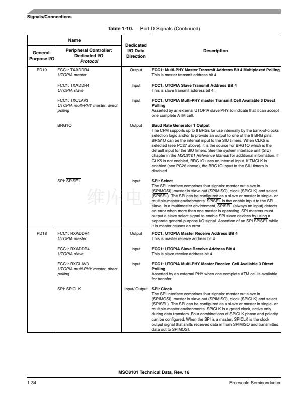
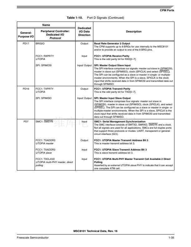
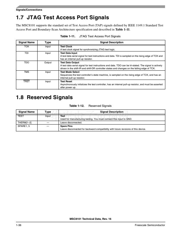
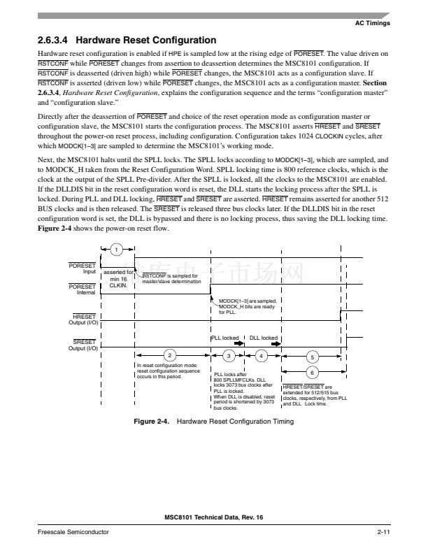
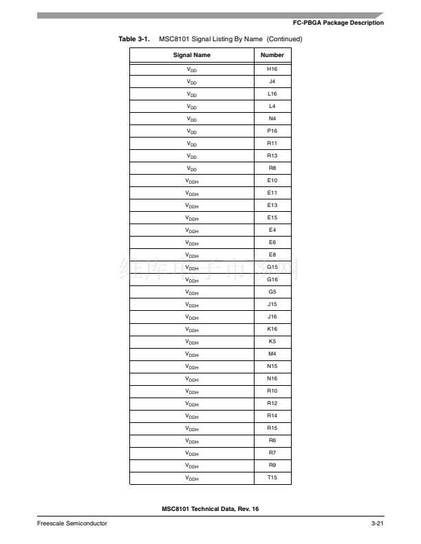
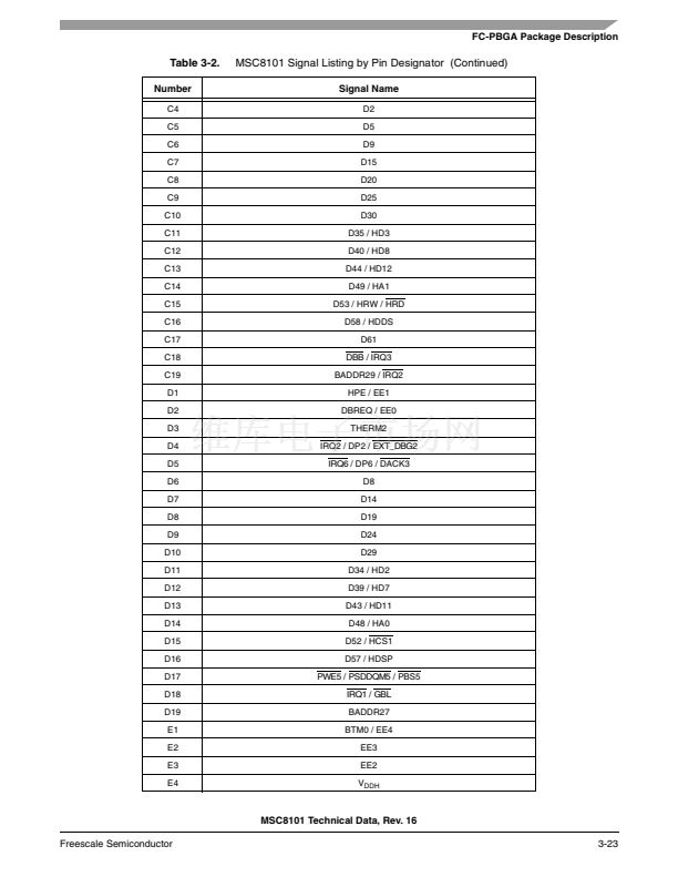
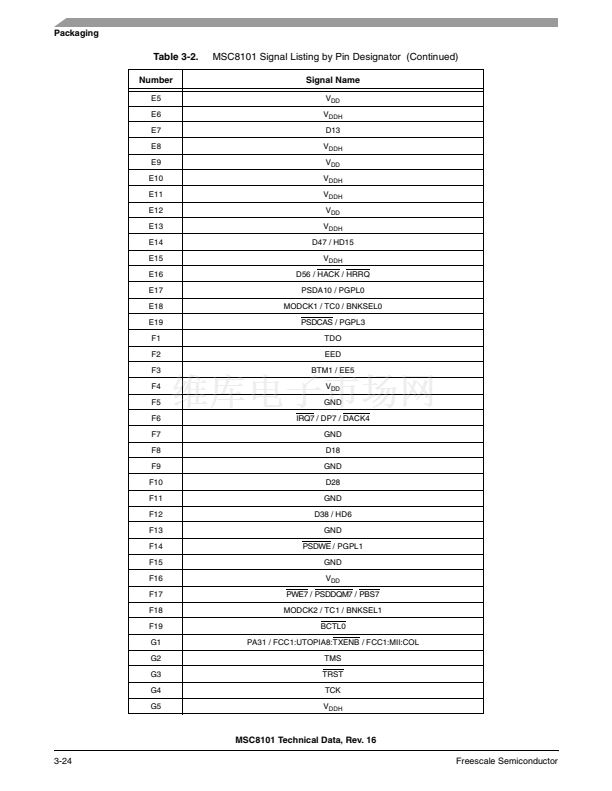
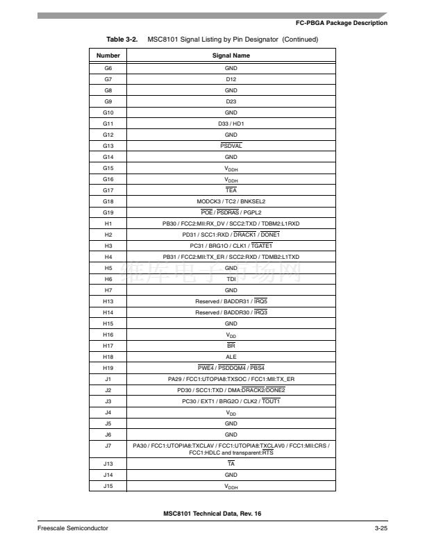
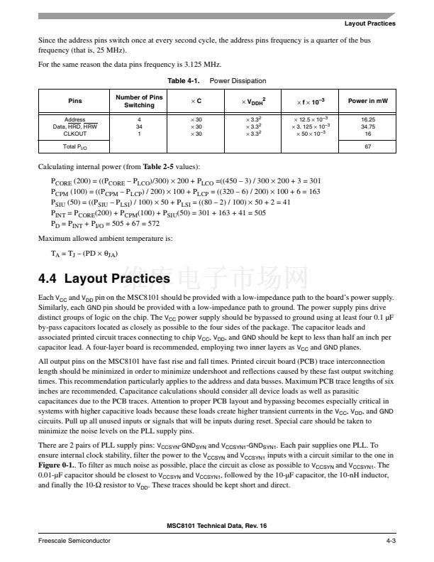
Design Considerations
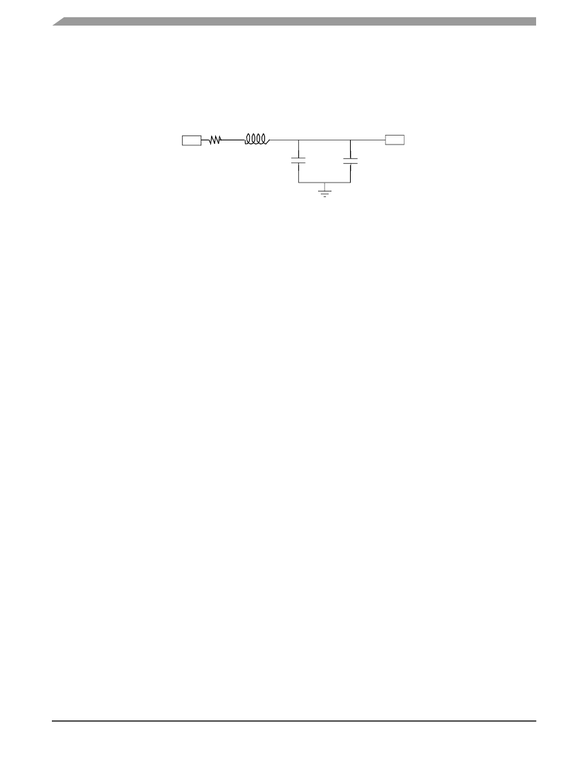
GND
SYN
and
GND
SYN1
should be provided with an extremely low impedance path to ground and should be bypassed
to
V
CCSYN
and
V
CCSYN1
, respectively, by a 0.01-碌F capacitor located as close as possible to the chip package. The
user should also bypass
GND
SYN
and
GND
SYN1
to
V
CCSYN
and
V
CCSYN1
with a 0.01-碌F capacitor as closely as
possible to the chip package
V
DD
10鈩?/div>
10nH
10 碌F
0.01 碌F
V
CCSYN
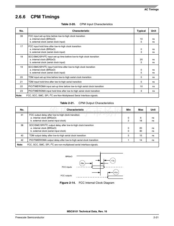
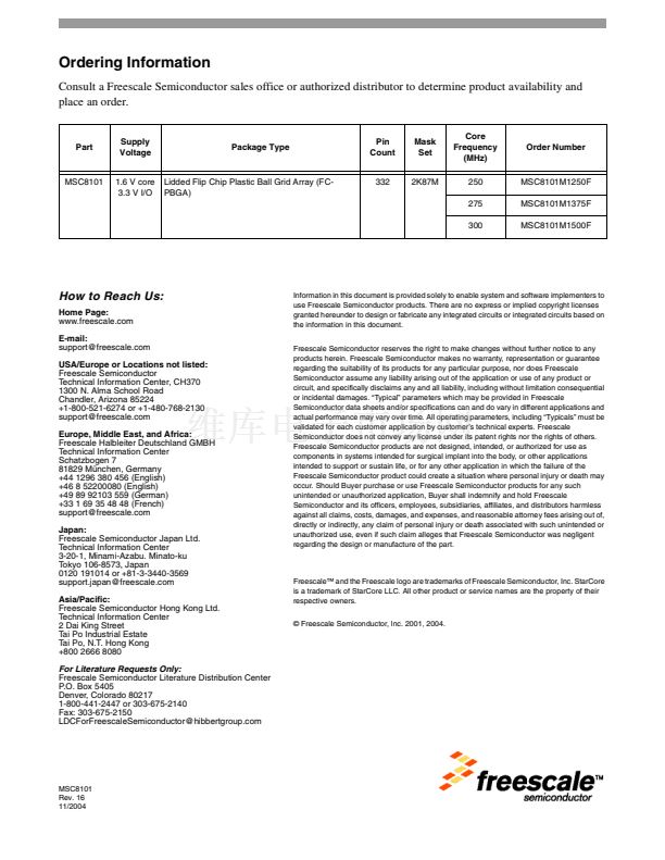
Figure 0-1.
VCCSYN and VCCSYN1 Bypass
MSC8101 Technical Data, Rev. 16
4-4
Freescale Semiconductor


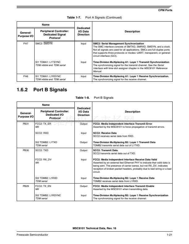
 1
1
 2
2
 3
3
 4
4
 5
5
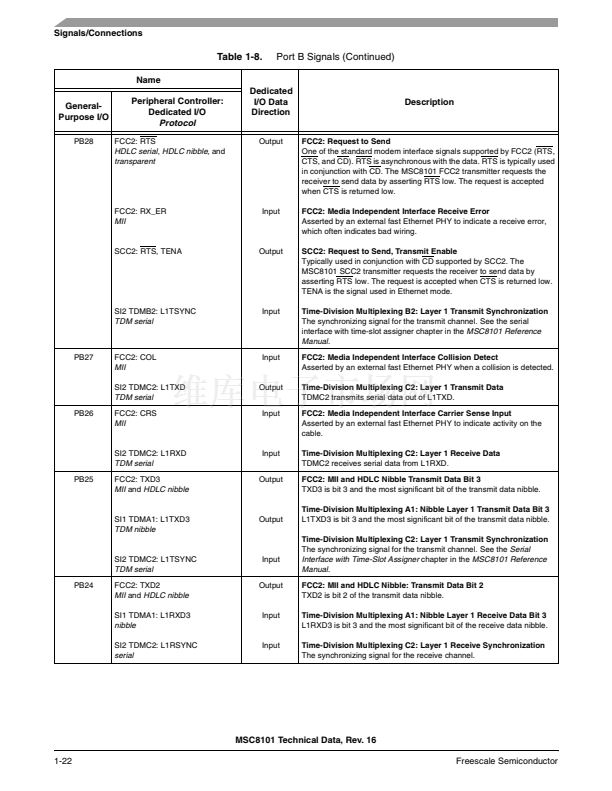
 6
6
 7
7
 8
8
 9
9
 10
10
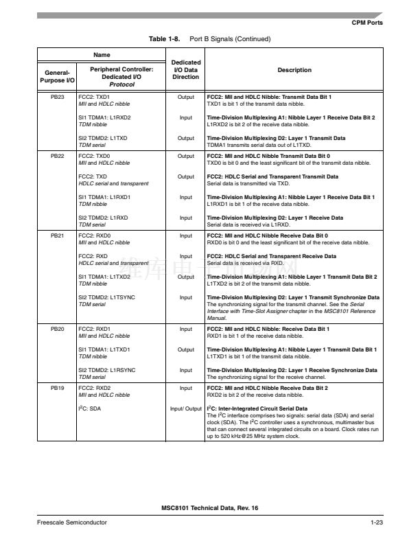
 11
11
 12
12
 13
13
 14
14
 15
15
 16
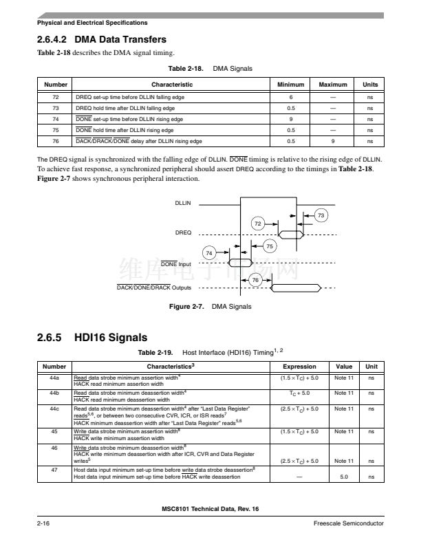
16
 17
17
 18
18
 19
19
 20
20
 21
21
 22
22
 23
23
 24
24
 25
25
 26
26
 27
27
 28
28
 29
29
 30
30
 31
31
 32
32
 33
33
 34
34
 35
35
 36
36
 37
37
 38
38
 39
39
 40
40
 41
41
 42
42
 43
43
 44
44
 45
45
 46
46
 47
47
 48
48
 49
49
 50
50
 51
51
 52
52
 53
53
 54
54
 55
55
 56
56
 57
57
 58
58
 59
59
 60
60
 61
61
 62
62
 63
63
 64
64
 65
65
 66
66
 67
67
 68
68
 69
69
 70
70
 71
71
 72
72
 73
73
 74
74
 75
75
 76
76
 77
77
 78
78
 79
79
 80
80
 81
81
 82
82
 83
83
 84
84
 85
85
 86
86
 87
87
 88
88
 89
89
 90
90
 91
91
 92
92
 93
93
 94
94
 95
95
 96
96
 97
97
 98
98
 99
99
 100
100
 101
101
 102
102
 103
103
 104
104
