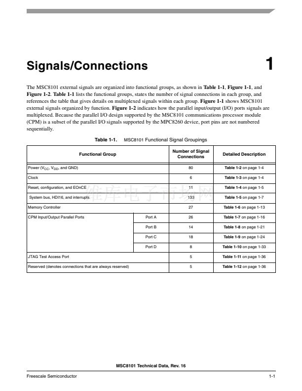
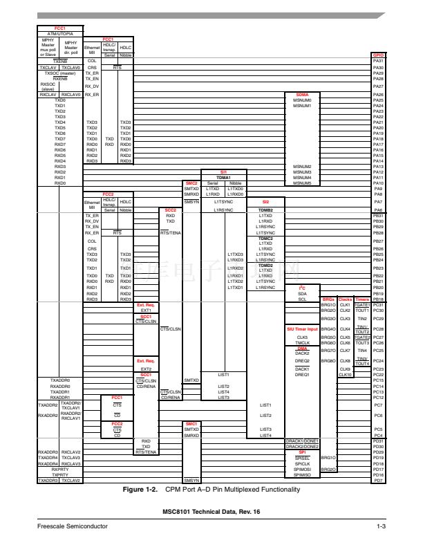
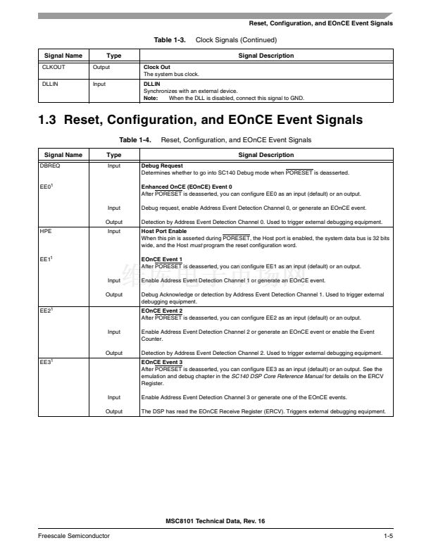
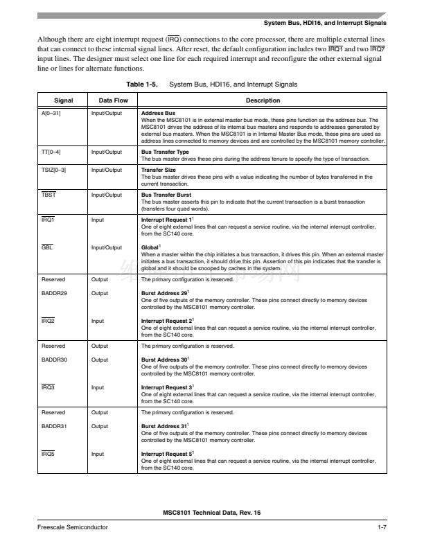
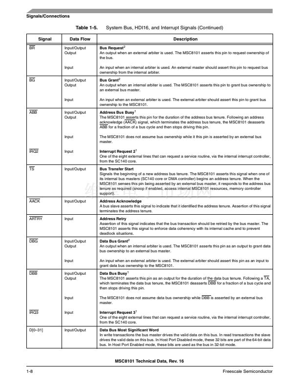
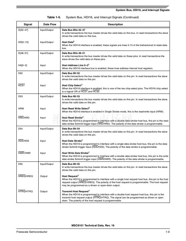
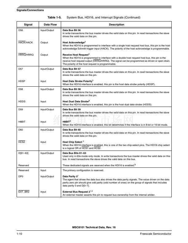
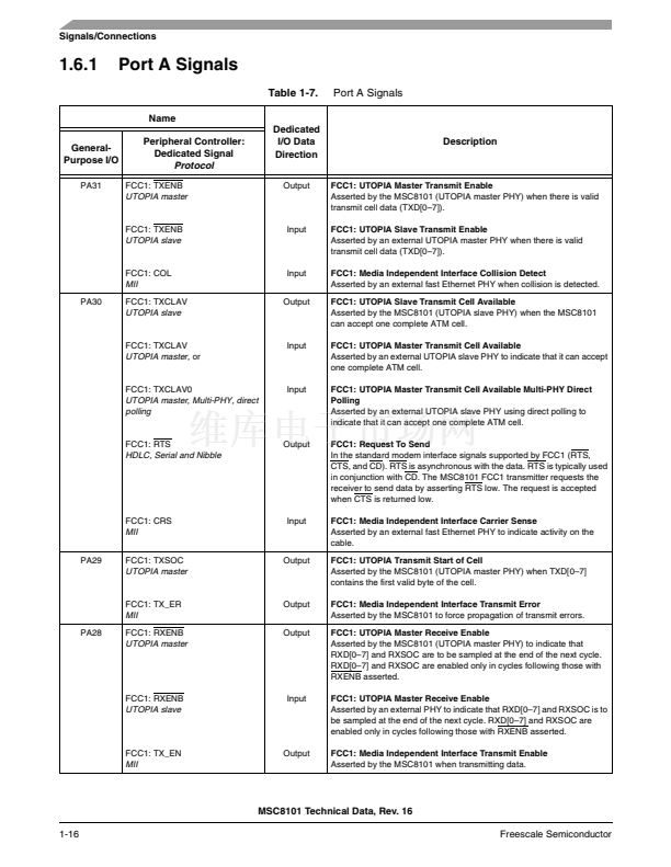
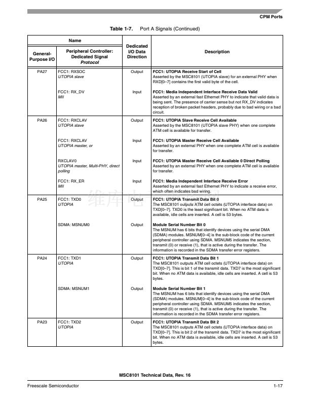
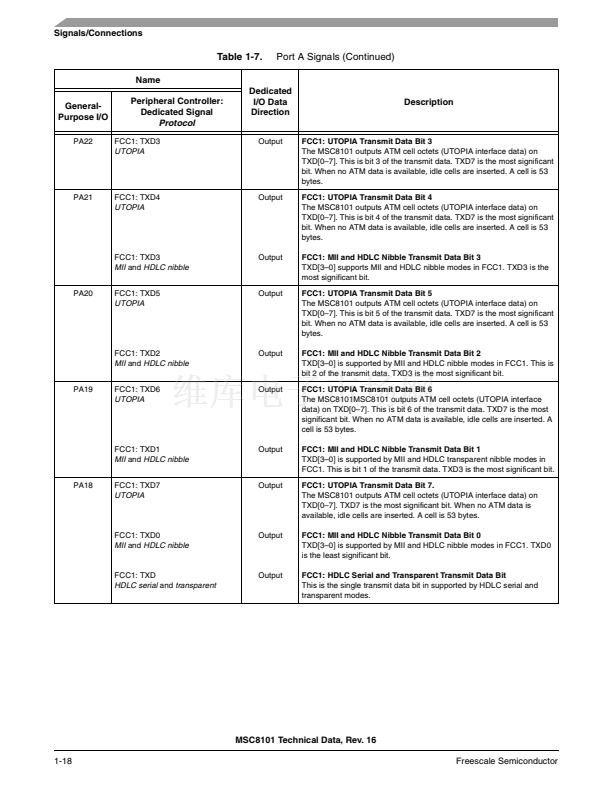
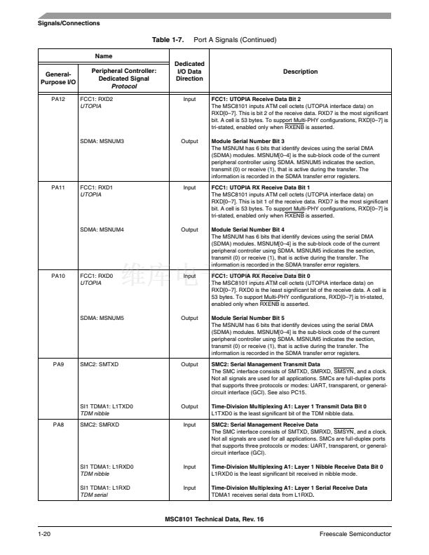
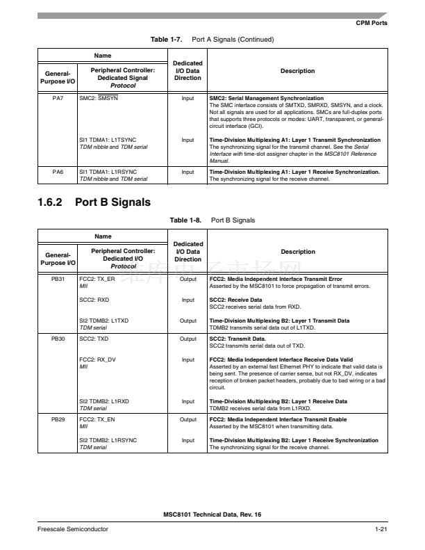
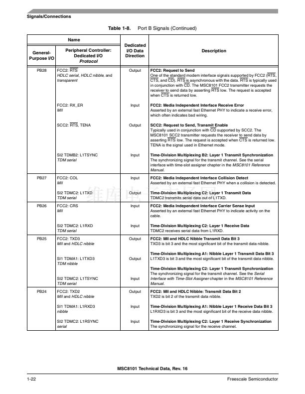
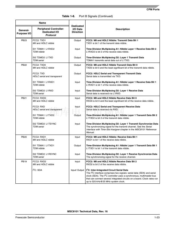
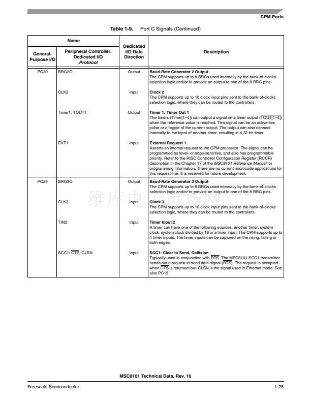
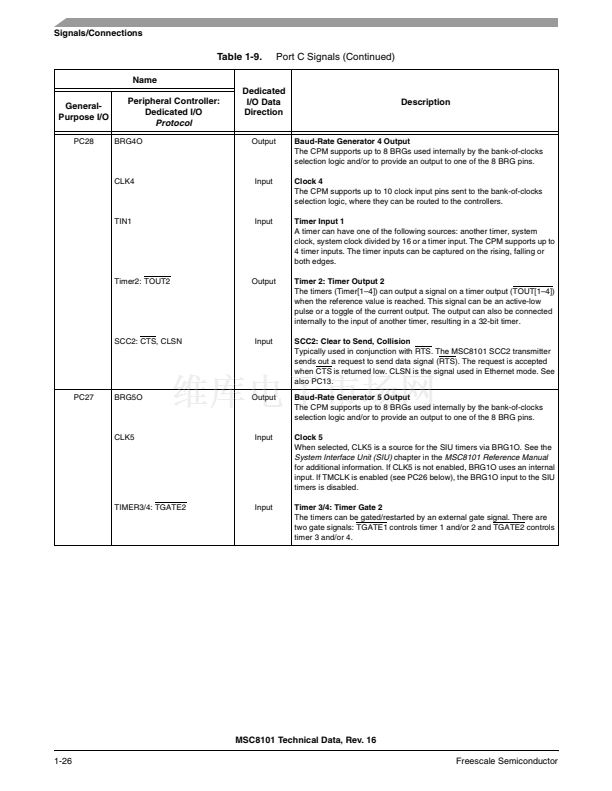
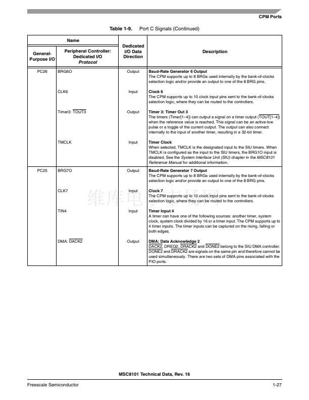
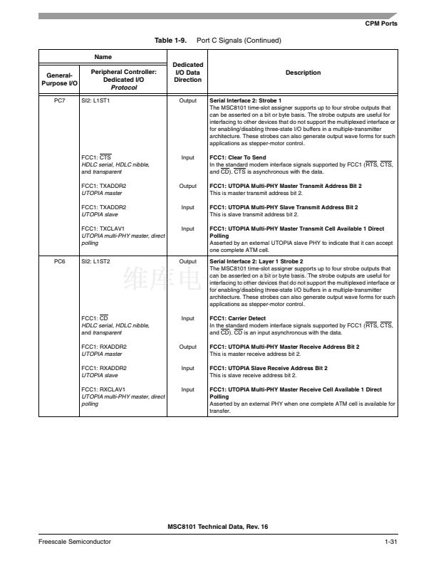
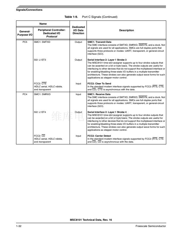
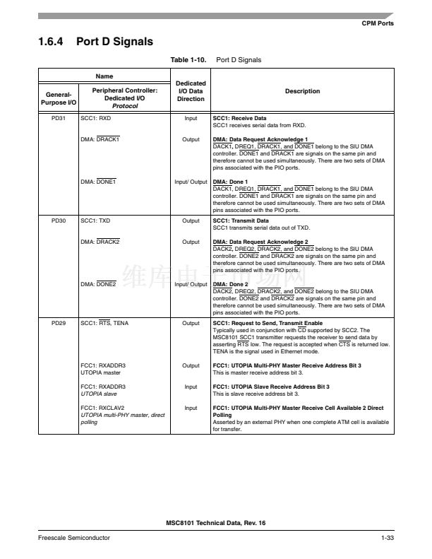
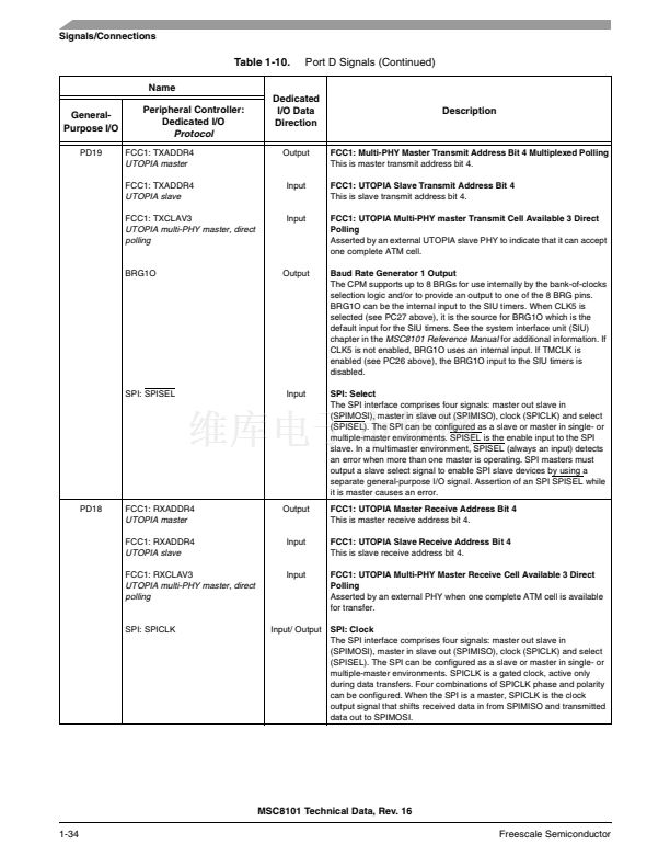
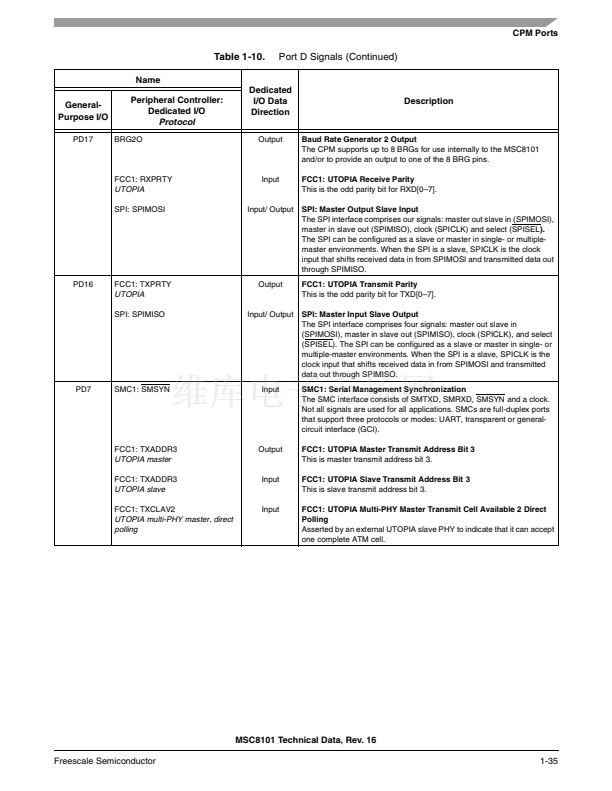
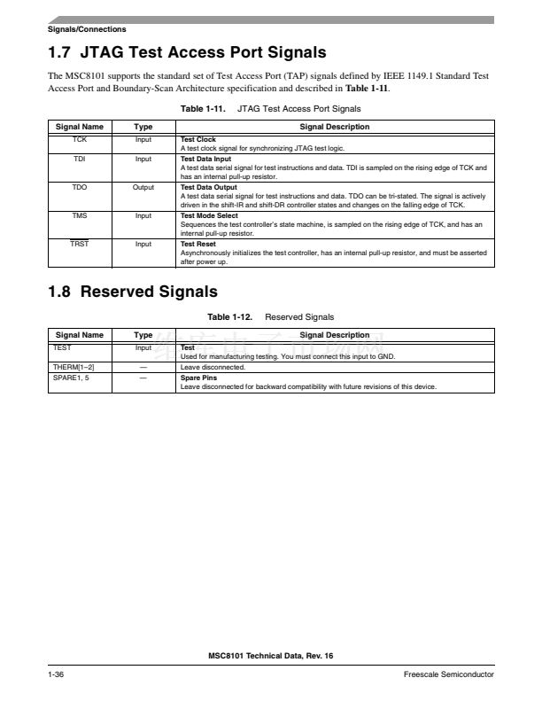
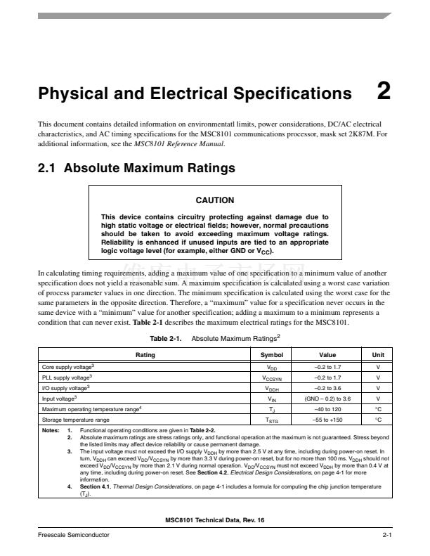
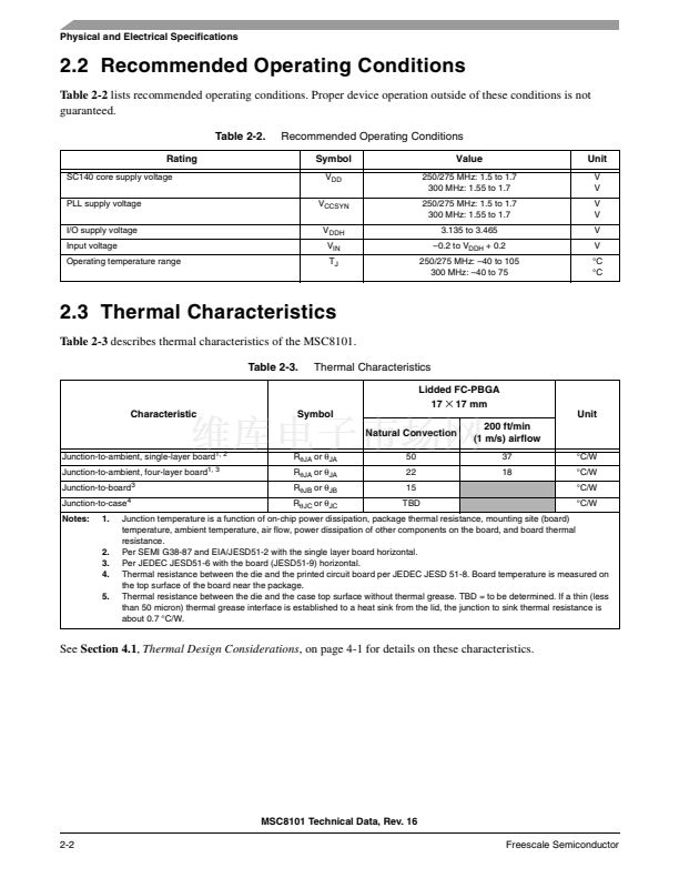
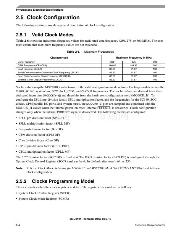
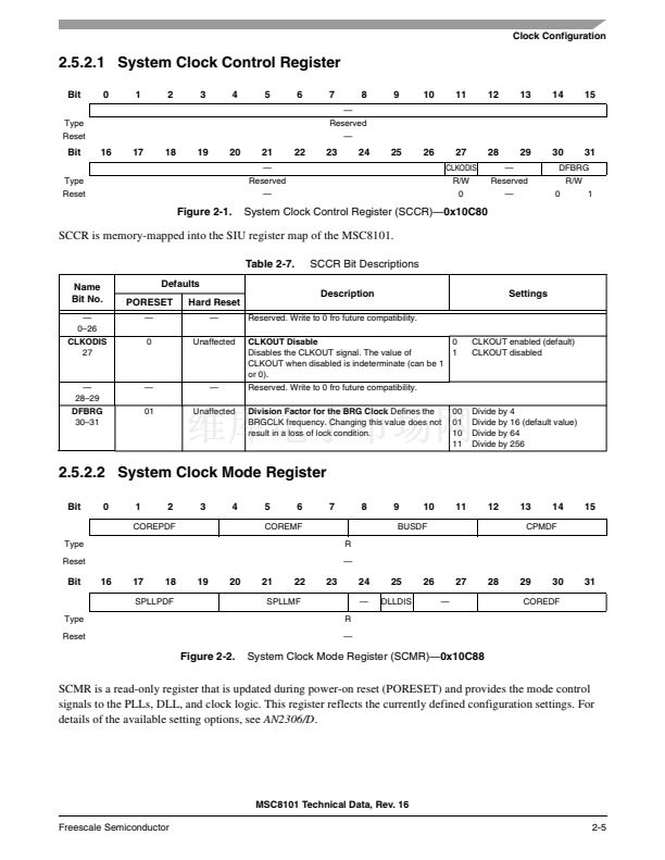
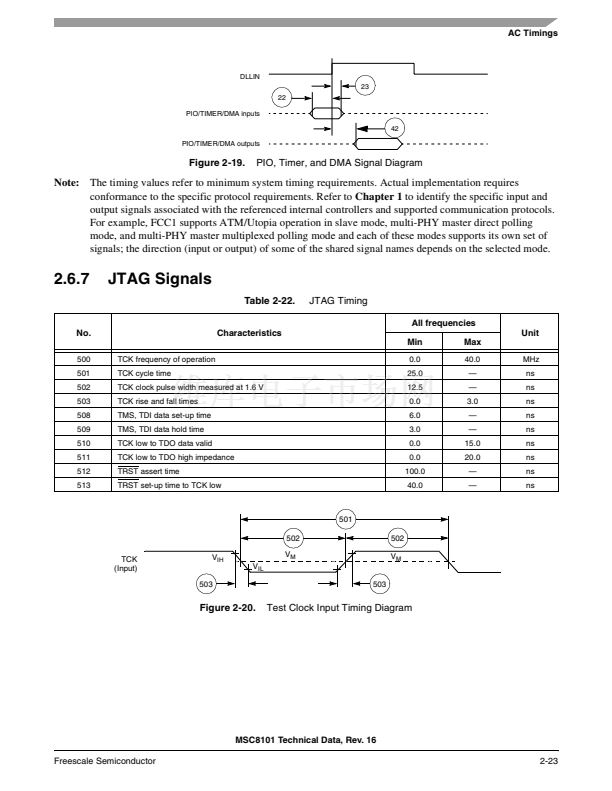
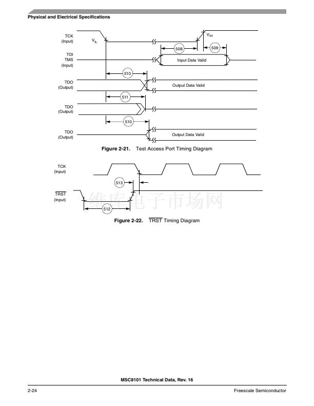
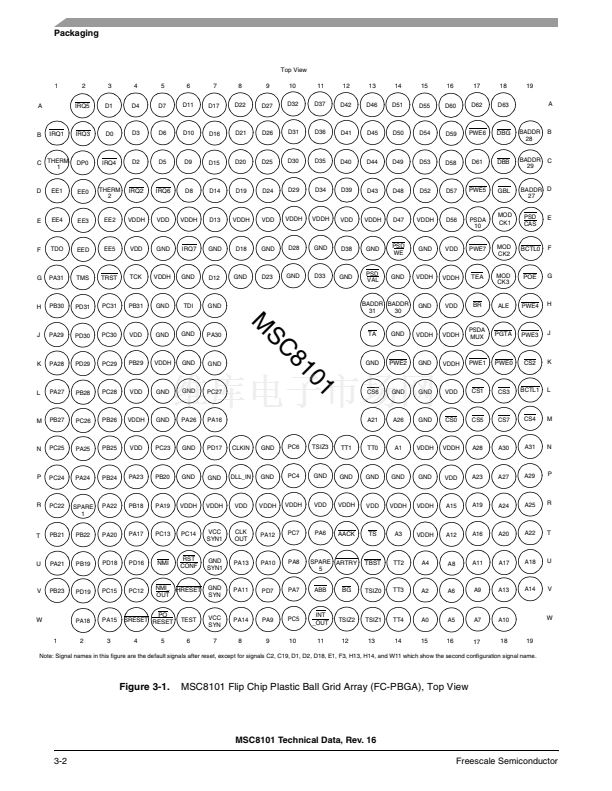
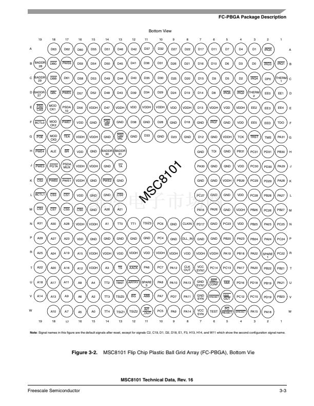
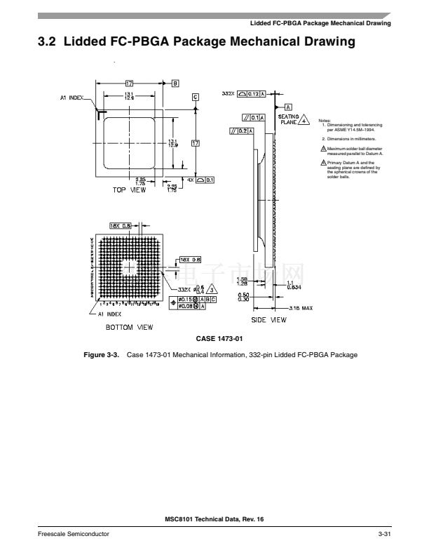
Packaging
3
This chapter provides information about the MSC8101 package, including diagrams of the package pinouts and
tables showing how the signals discussed in
Chapter 1
are allocated. The MSC8101 is available in a 332-pin
lidded flip chip-plastic ball grid array (FC-PBGA).
3.1 FC-PBGA Package Description
Figure 3-1
and
Figure 3-2
show top and bottom views of the FC-PBGA package, including pinouts.
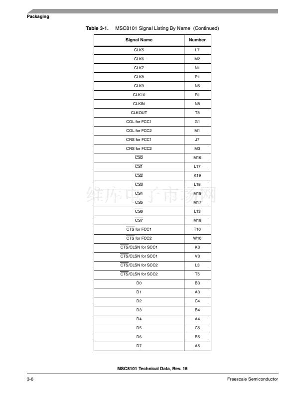
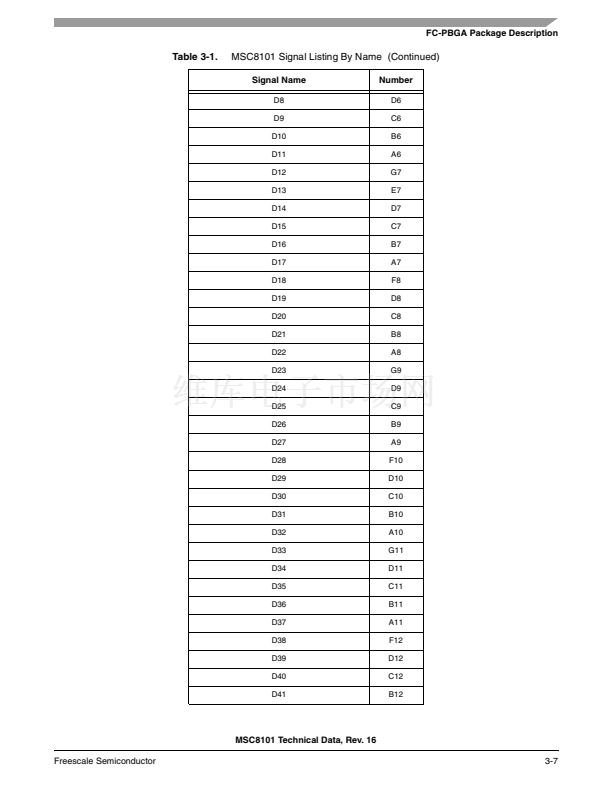
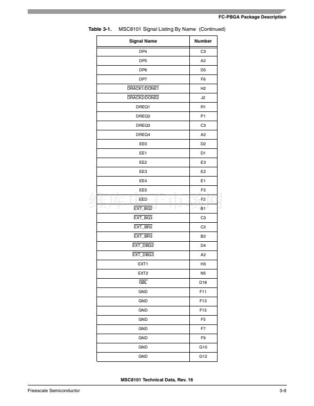
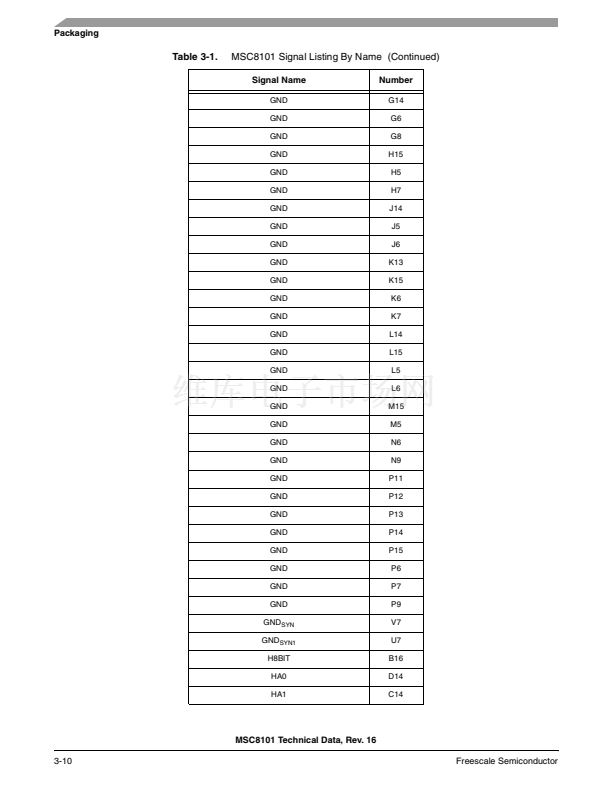
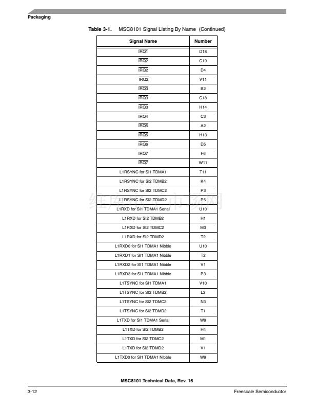
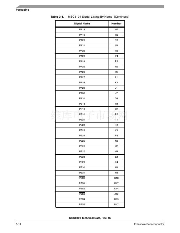
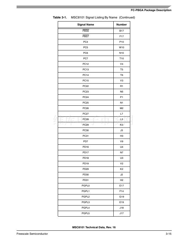
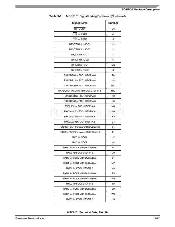
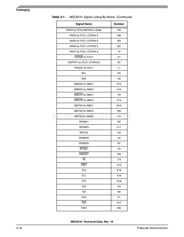
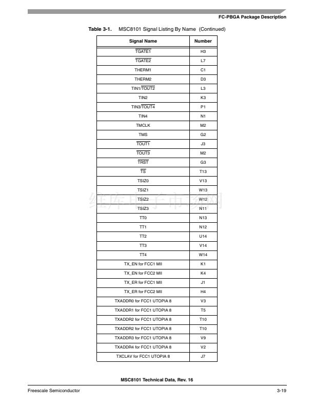
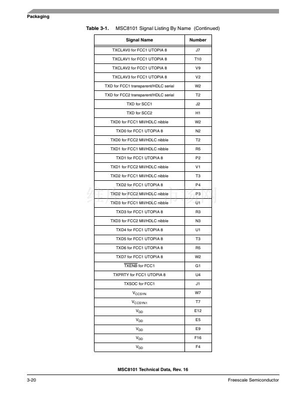
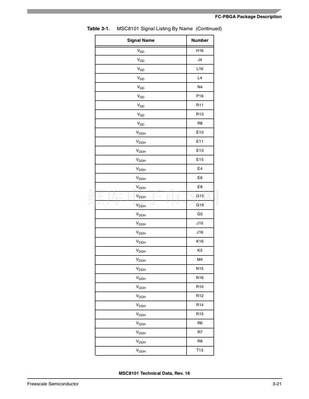
Table 3-1
lists
the MSC8101 signals alphabetically by signal name. Connections with multiple names are listed individually by
each name. Signals with programmable polarity are shown both as signals which are asserted low (default) and
high (that is,
NAME
/
NAME
).
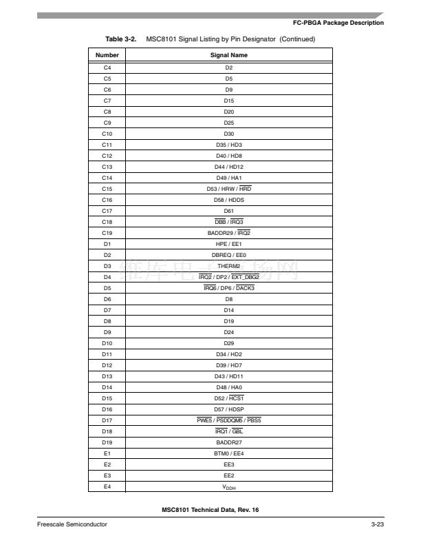
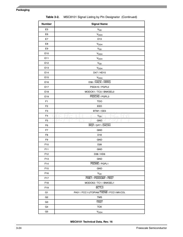
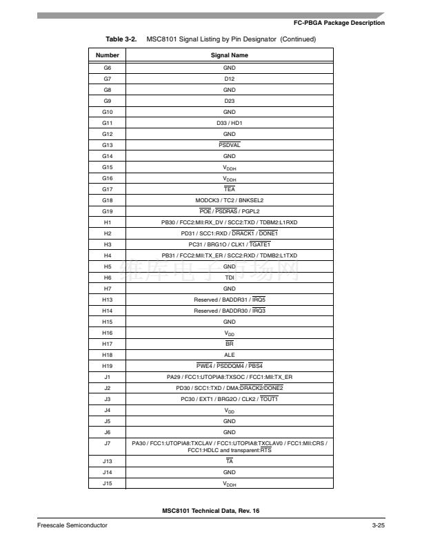
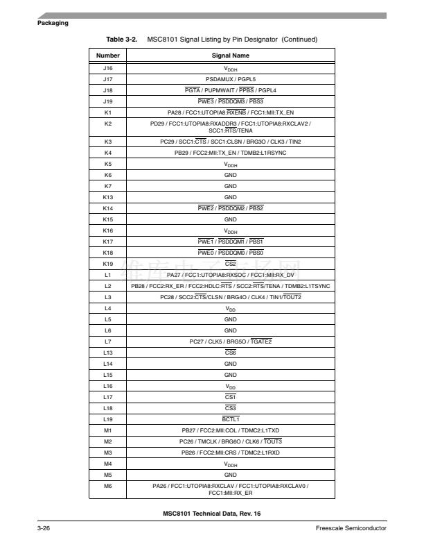
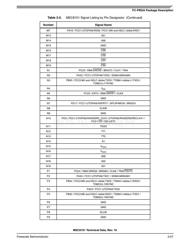
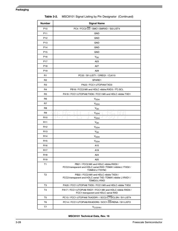
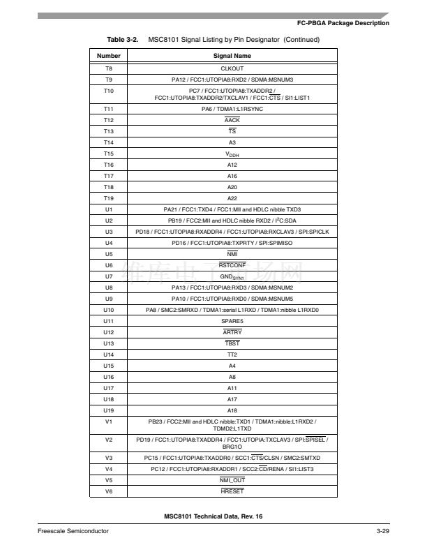
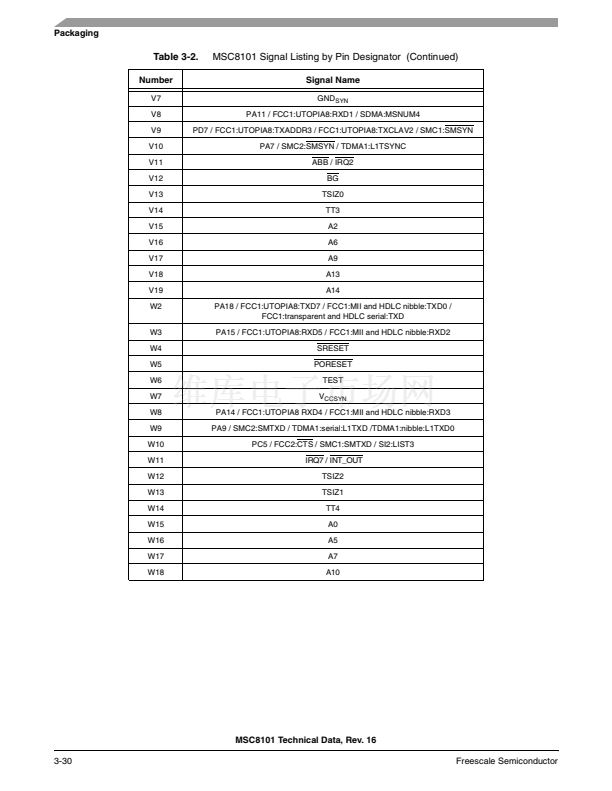
Table 3-2
lists the signals numerically by pin number. Each pin number is listed once
with the various signals that are multiplexed to it. For simplicity, signals with programmable polarity are shown in
this table only with their default name (asserted low).
MSC8101 Technical Data, Rev. 16
Freescale Semiconductor
3-1


 1
1
 2
2
 3
3
 4
4
 5
5
 6
6
 7
7
 8
8
 9
9
 10
10
 11
11
 12
12
 13
13
 14
14
 15
15
 16
16
 17
17
 18
18
 19
19
 20
20
 21
21
 22
22
 23
23
 24
24
 25
25
 26
26
 27
27
 28
28
 29
29
 30
30
 31
31
 32
32
 33
33
 34
34
 35
35
 36
36
 37
37
 38
38
 39
39
 40
40
 41
41
 42
42
 43
43
 44
44
 45
45
 46
46
 47
47
 48
48
 49
49
 50
50
 51
51
 52
52
 53
53
 54
54
 55
55
 56
56
 57
57
 58
58
 59
59
 60
60
 61
61
 62
62
 63
63
 64
64
 65
65
 66
66
 67
67
 68
68
 69
69
 70
70
 71
71
 72
72
 73
73
 74
74
 75
75
 76
76
 77
77
 78
78
 79
79
 80
80
 81
81
 82
82
 83
83
 84
84
 85
85
 86
86
 87
87
 88
88
 89
89
 90
90
 91
91
 92
92
 93
93
 94
94
 95
95
 96
96
 97
97
 98
98
 99
99
 100
100
 101
101
 102
102
 103
103
 104
104
