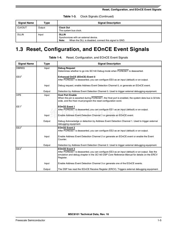
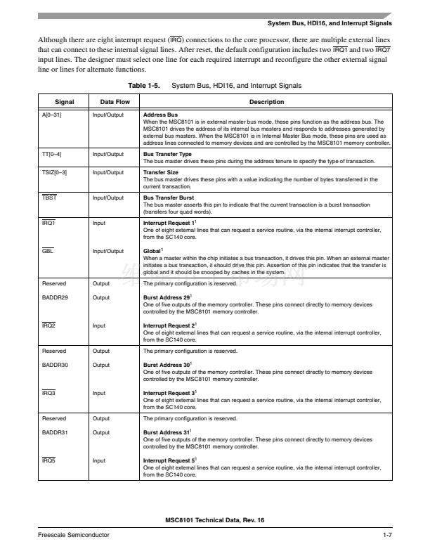
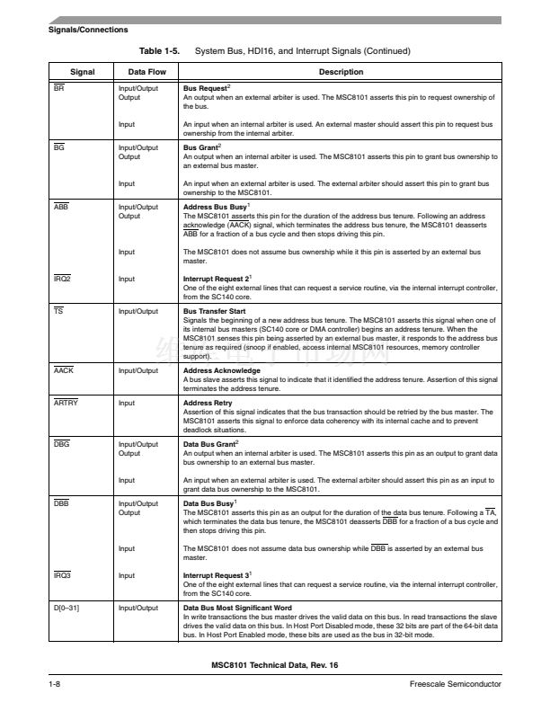
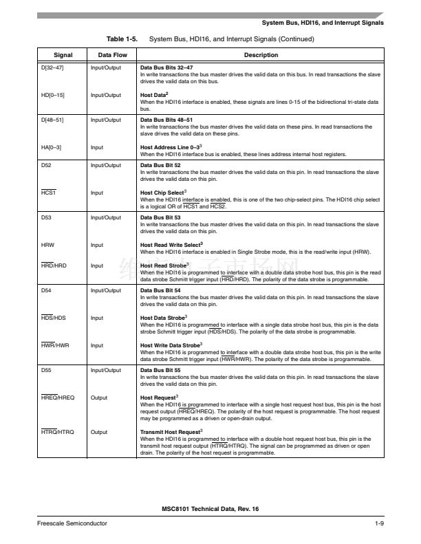
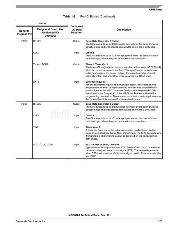
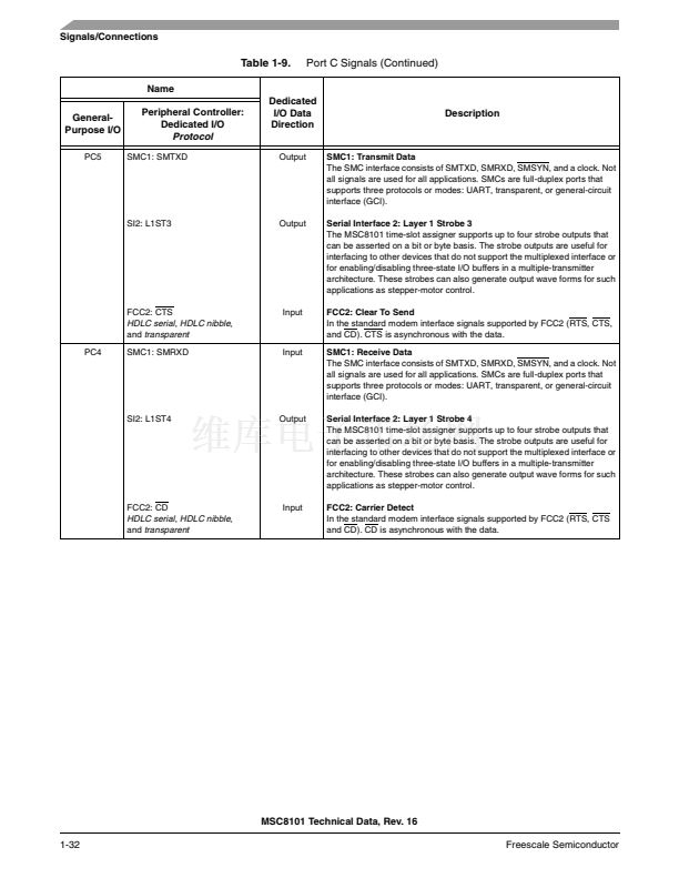
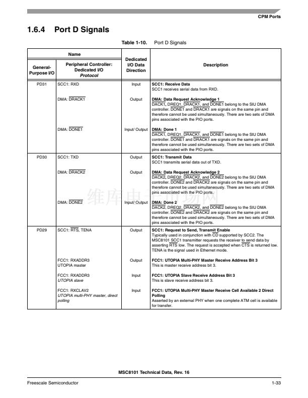
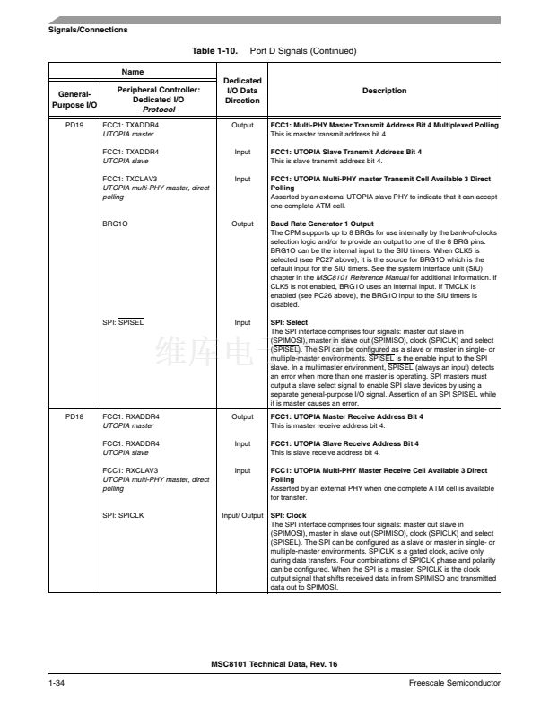
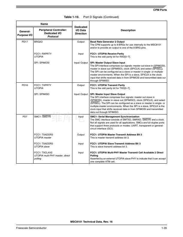
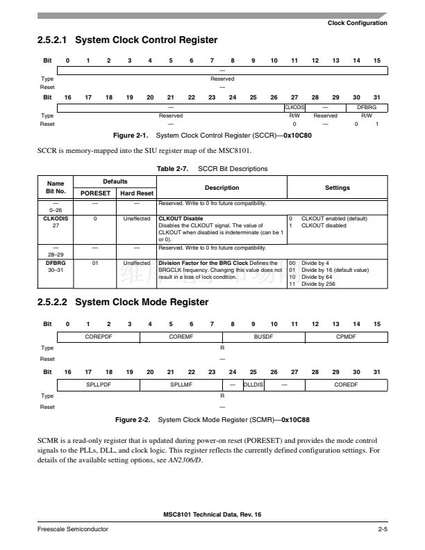
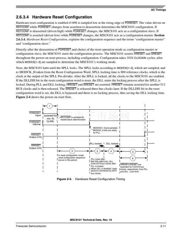
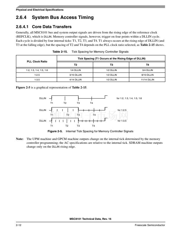
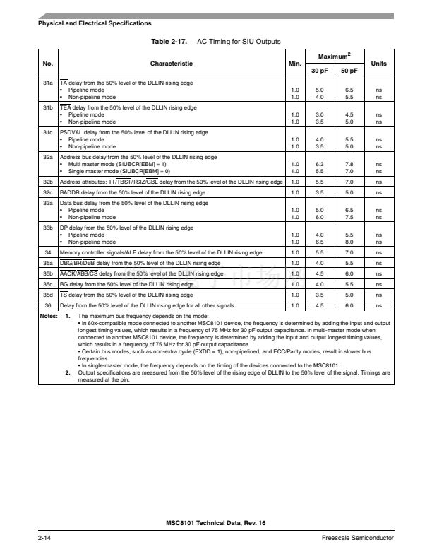
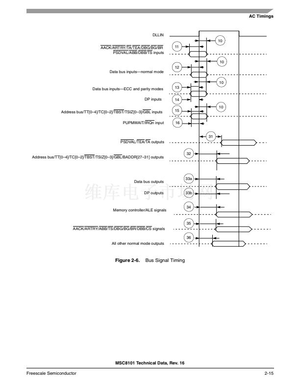
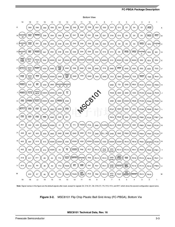
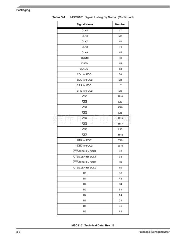
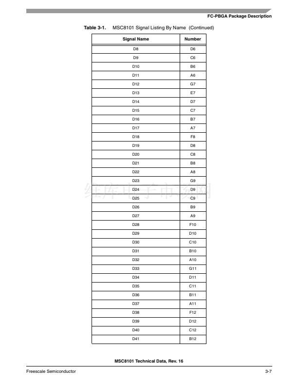
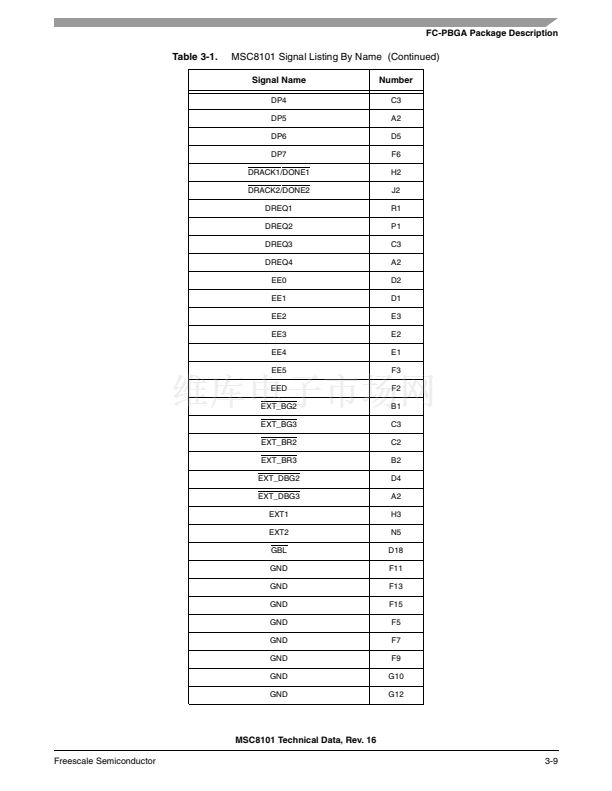
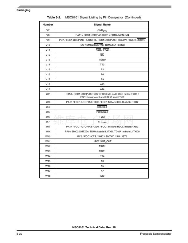
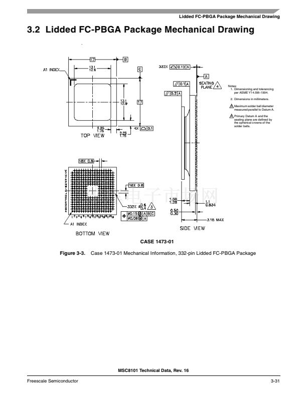
Physical and Electrical Specifications
2
This document contains detailed information on environmentatl limits, power considerations, DC/AC electrical
characteristics, and AC timing specifications for the MSC8101 communications processor, mask set 2K87M. For
additional information, see the
MSC8101 Reference Manual.
2.1 Absolute Maximum Ratings
CAUTION
This device contains circuitry protecting against damage due to
high static voltage or electrical fields; however, normal precautions
should be taken to avoid exceeding maximum voltage ratings.
Reliability is enhanced if unused inputs are tied to an appropriate
logic voltage level (for example, either GND or V
CC
).
In calculating timing requirements, adding a maximum value of one specification to a minimum value of another
specification does not yield a reasonable sum. A maximum specification is calculated using a worst case variation
of process parameter values in one direction. The minimum specification is calculated using the worst case for the
same parameters in the opposite direction. Therefore, a 鈥渕aximum鈥?value for a specification never occurs in the
same device with a 鈥渕inimum鈥?value for another specification; adding a maximum to a minimum represents a
condition that can never exist.
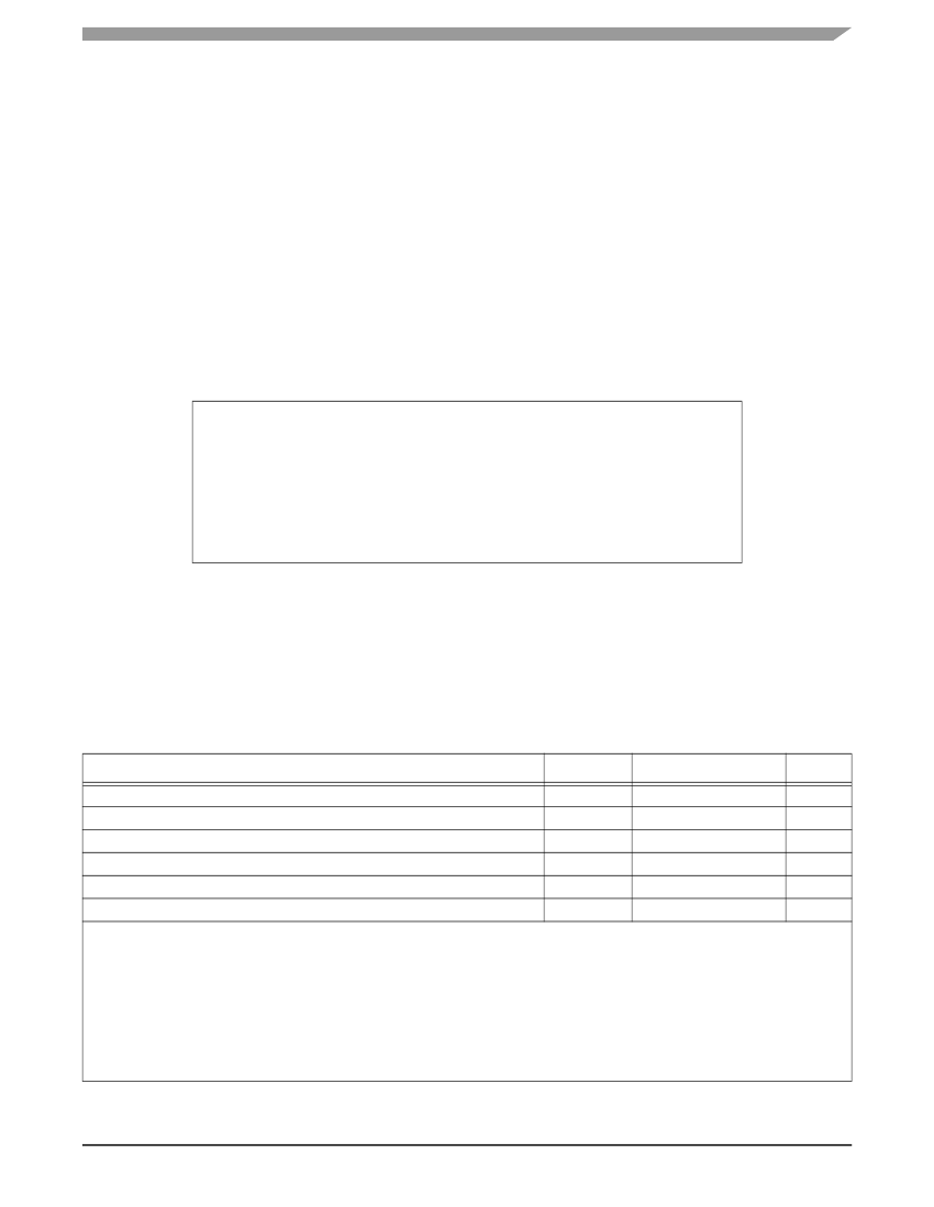
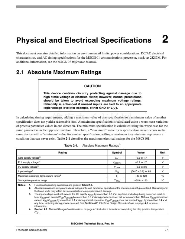
Table 2-1
describes the maximum electrical ratings for the MSC8101.
Table 2-1.
Rating
Core supply voltage
3
PLL supply voltage
3
I/O supply voltage
3
Input voltage
3
Maximum operating temperature range
4
Storage temperature range
Notes:
1.
2.
3.
Absolute Maximum Ratings
2
Symbol
V
DD
V
CCSYN
V
DDH
V
IN
T
J
T
STG
Value
鈥?.2 to 1.7
鈥?.2 to 1.7
鈥?.2 to 3.6
(GND 鈥?0.2) to 3.6
鈥?0 to 120
鈥?5 to +150
Unit
V
V
V
V
掳C
掳C
4.
Functional operating conditions are given in
Table 2-2.
Absolute maximum ratings are stress ratings only, and functional operation at the maximum is not guaranteed. Stress beyond
the listed limits may affect device reliability or cause permanent damage.
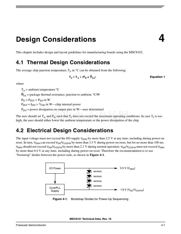
The input voltage must not exceed the I/O supply V
DDH
by more than 2.5 V at any time, including during power-on reset. In
turn, V
DDH
can exceed V
DD
/V
CCSYN
by more than 3.3 V during power-on reset, but for no more than 100 ms. V
DDH
should not
exceed V
DD
/V
CCSYN
by more than 2.1 V during normal operation. V
DD
/V
CCSYN
must not exceed V
DDH
by more than 0.4 V at
any time, including during power-on reset. See
Section 4.2,
Electrical Design Considerations,
on page 4-1 for more
information.
Section 4.1,
Thermal Design Considerations,
on page 4-1 includes a formula for computing the chip junction temperature
(T
J
).
MSC8101 Technical Data, Rev. 16
Freescale Semiconductor
2-1


 1
1
 2
2
 3
3
 4
4
 5
5
 6
6
 7
7
 8
8
 9
9
 10
10
 11
11
 12
12
 13
13
 14
14
 15
15
 16
16
 17
17
 18
18
 19
19
 20
20
 21
21
 22
22
 23
23
 24
24
 25
25
 26
26
 27
27
 28
28
 29
29
 30
30
 31
31
 32
32
 33
33
 34
34
 35
35
 36
36
 37
37
 38
38
 39
39
 40
40
 41
41
 42
42
 43
43
 44
44
 45
45
 46
46
 47
47
 48
48
 49
49
 50
50
 51
51
 52
52
 53
53
 54
54
 55
55
 56
56
 57
57
 58
58
 59
59
 60
60
 61
61
 62
62
 63
63
 64
64
 65
65
 66
66
 67
67
 68
68
 69
69
 70
70
 71
71
 72
72
 73
73
 74
74
 75
75
 76
76
 77
77
 78
78
 79
79
 80
80
 81
81
 82
82
 83
83
 84
84
 85
85
 86
86
 87
87
 88
88
 89
89
 90
90
 91
91
 92
92
 93
93
 94
94
 95
95
 96
96
 97
97
 98
98
 99
99
 100
100
 101
101
 102
102
 103
103
 104
104
