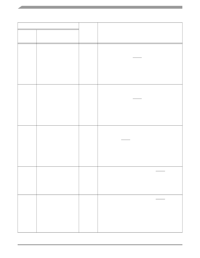
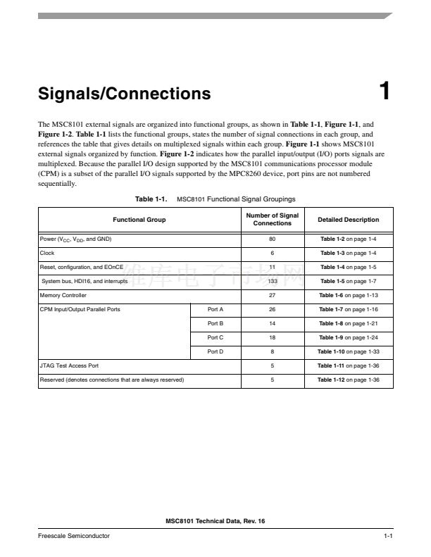
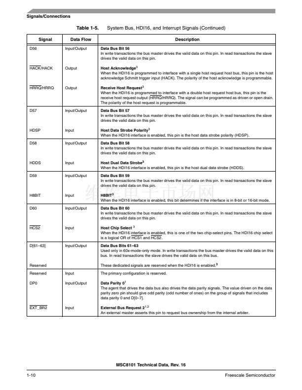
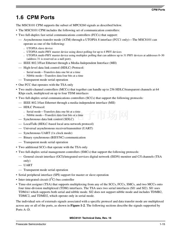
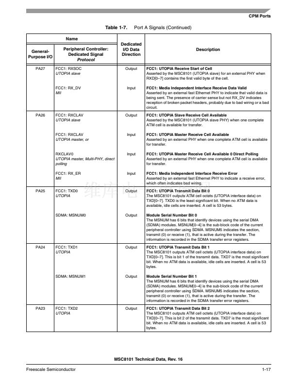
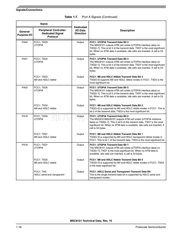
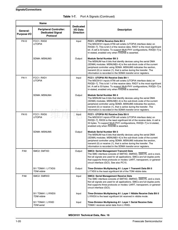
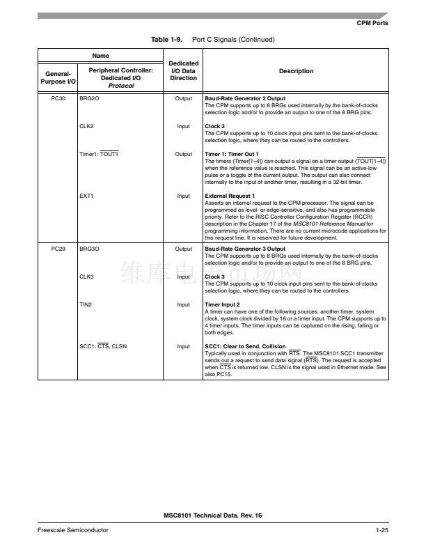
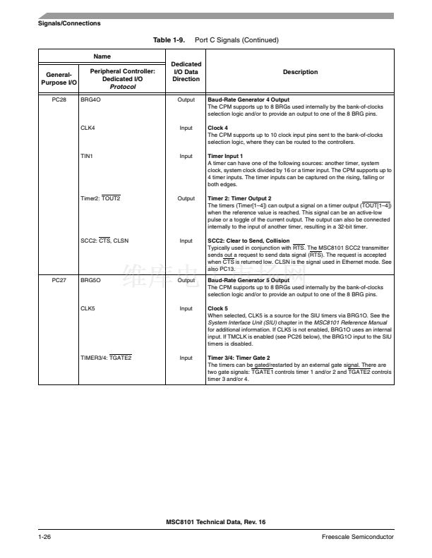
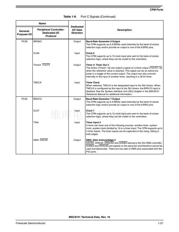
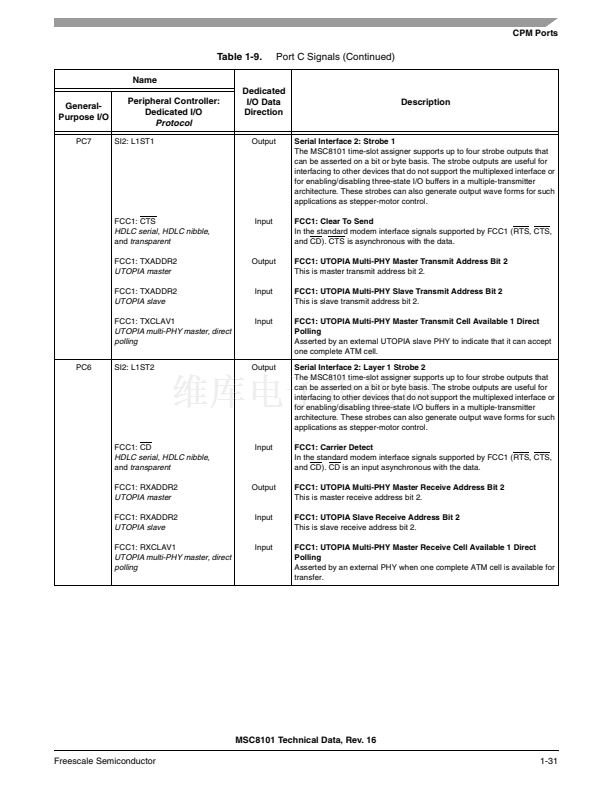
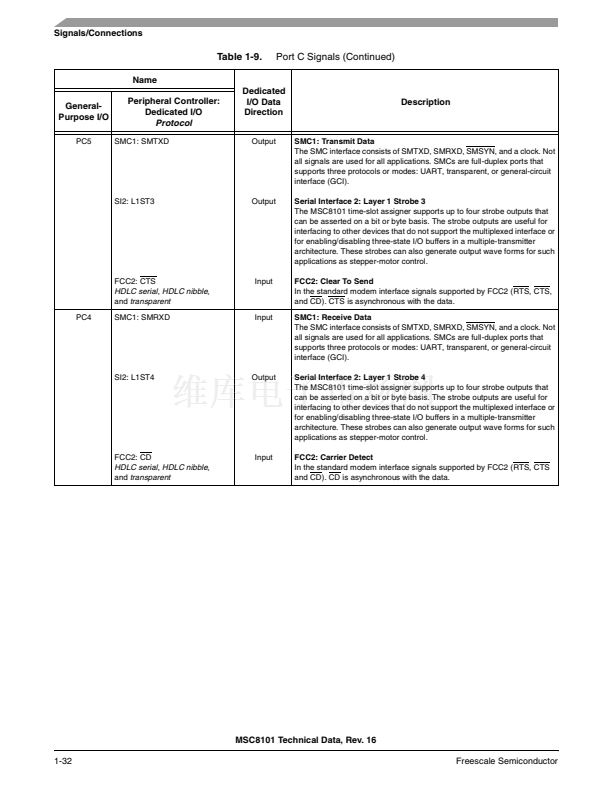
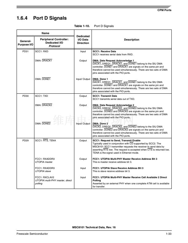
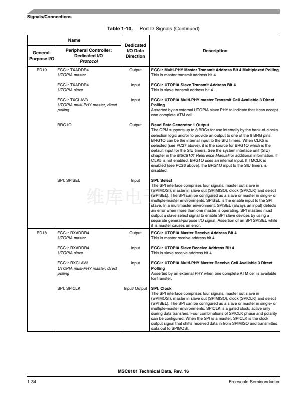
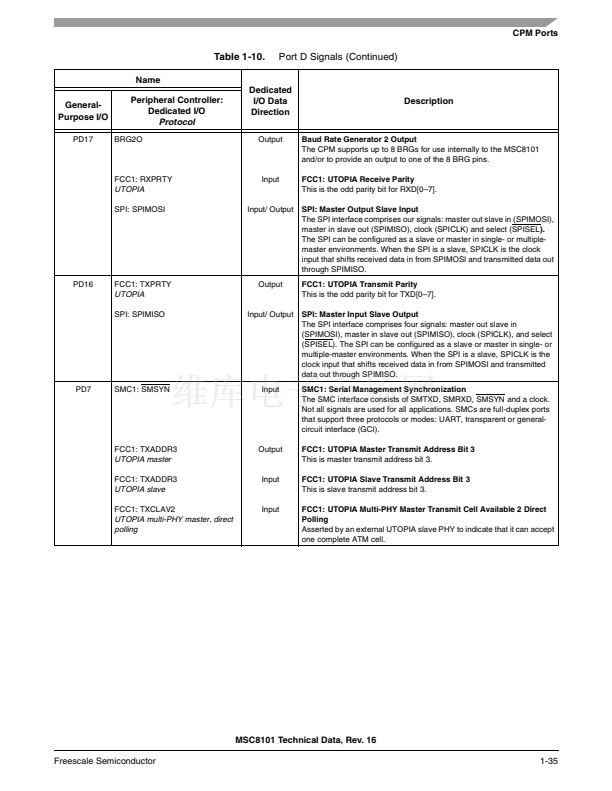
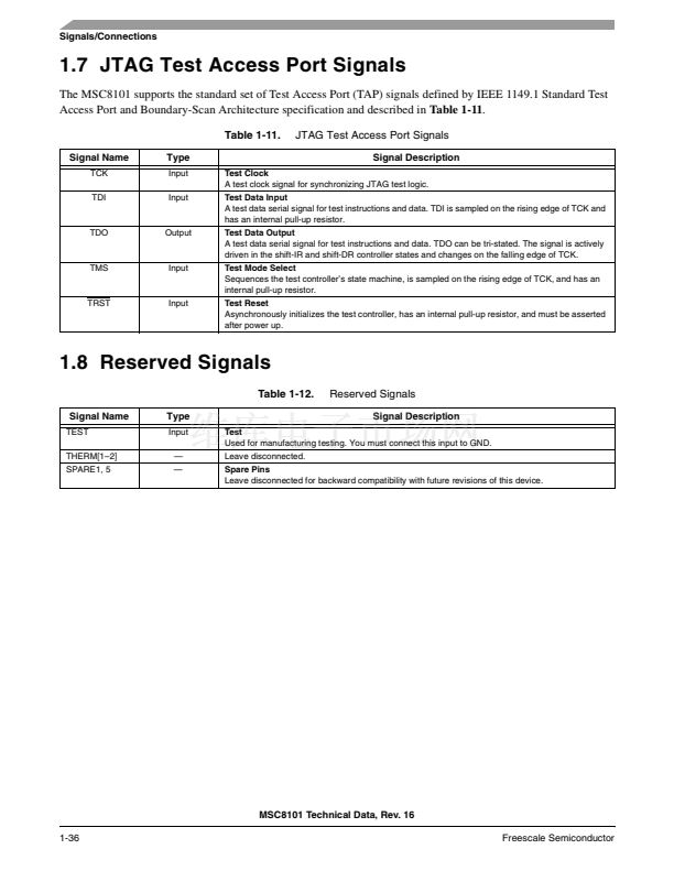
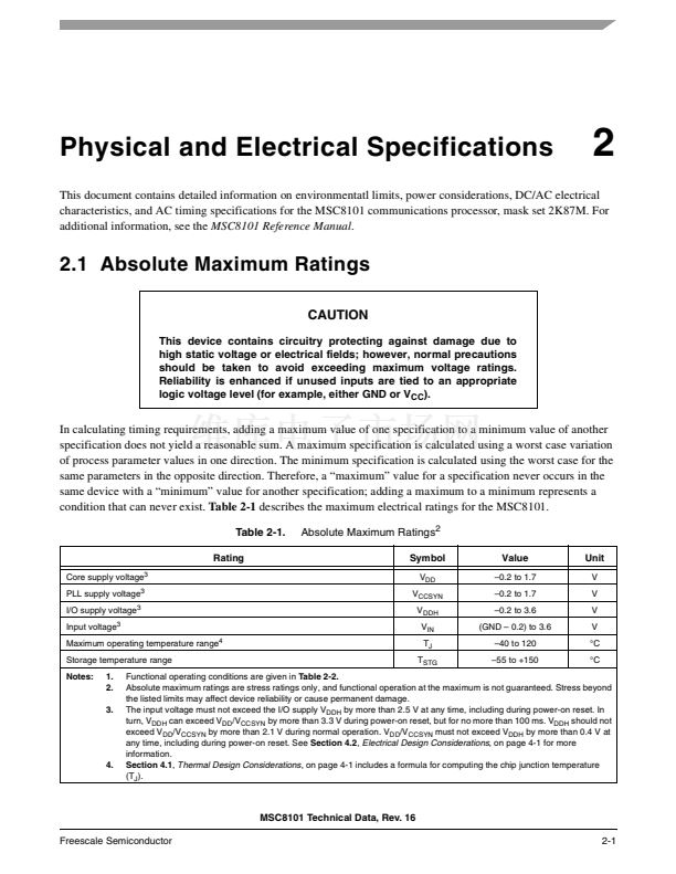
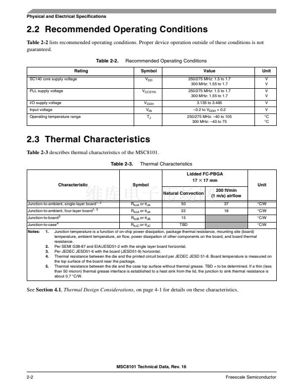
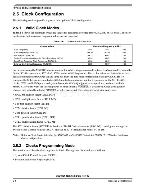
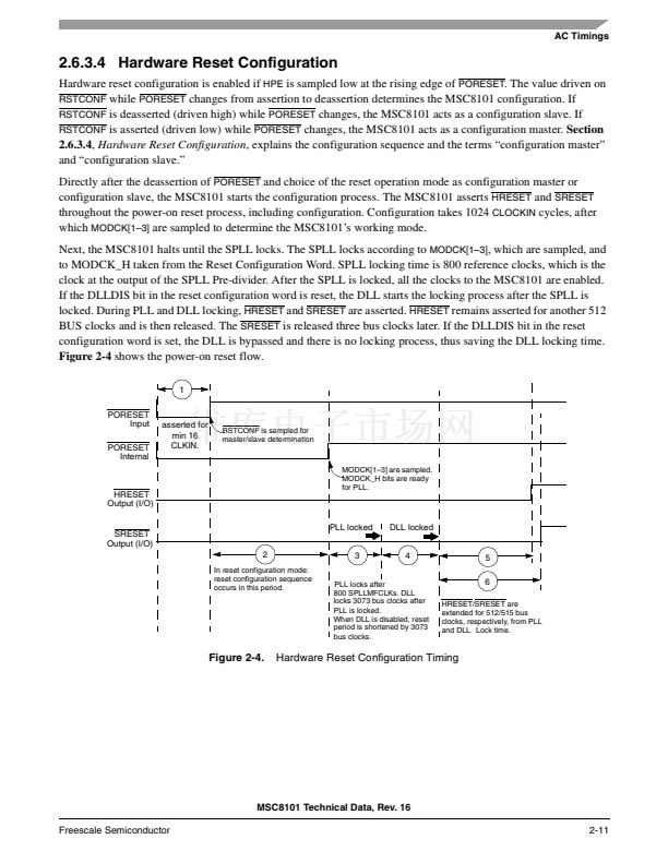
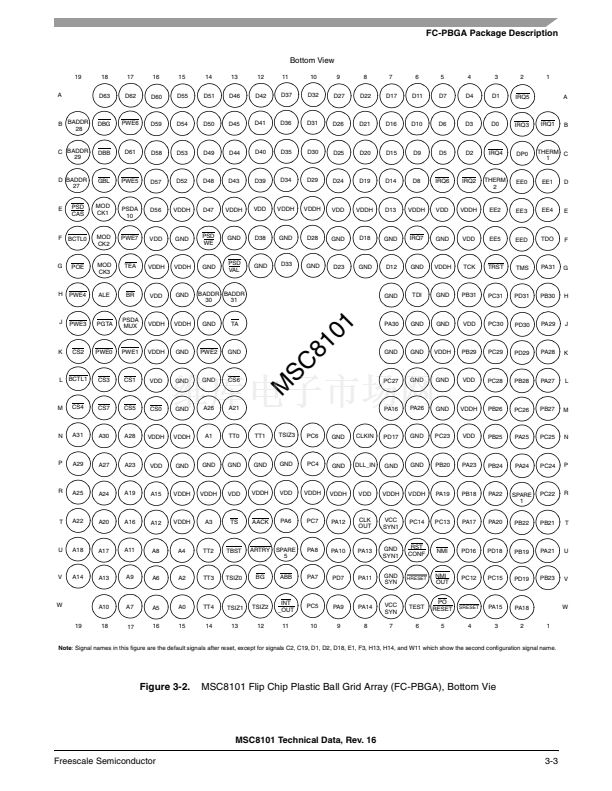
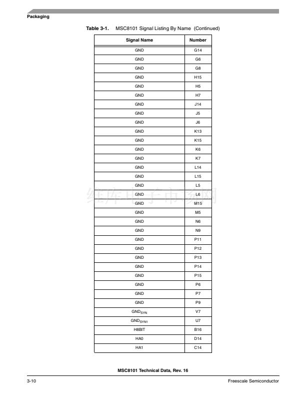
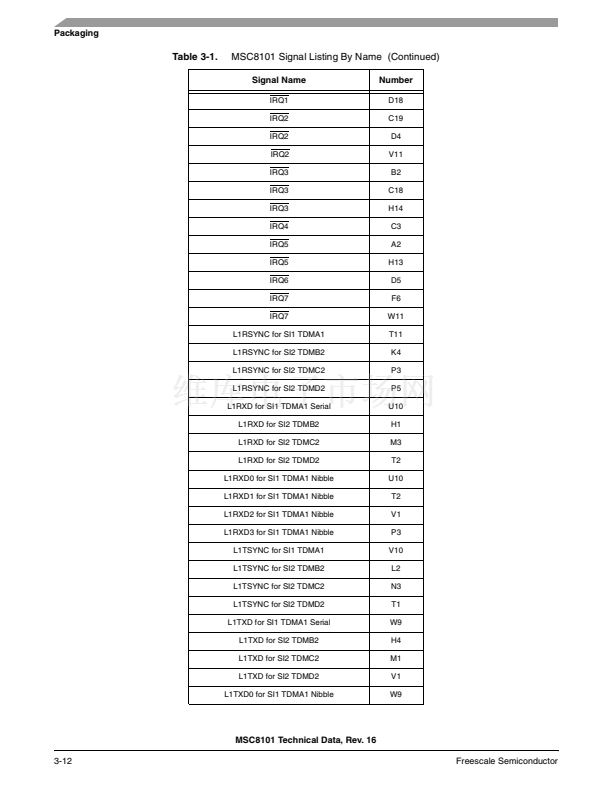
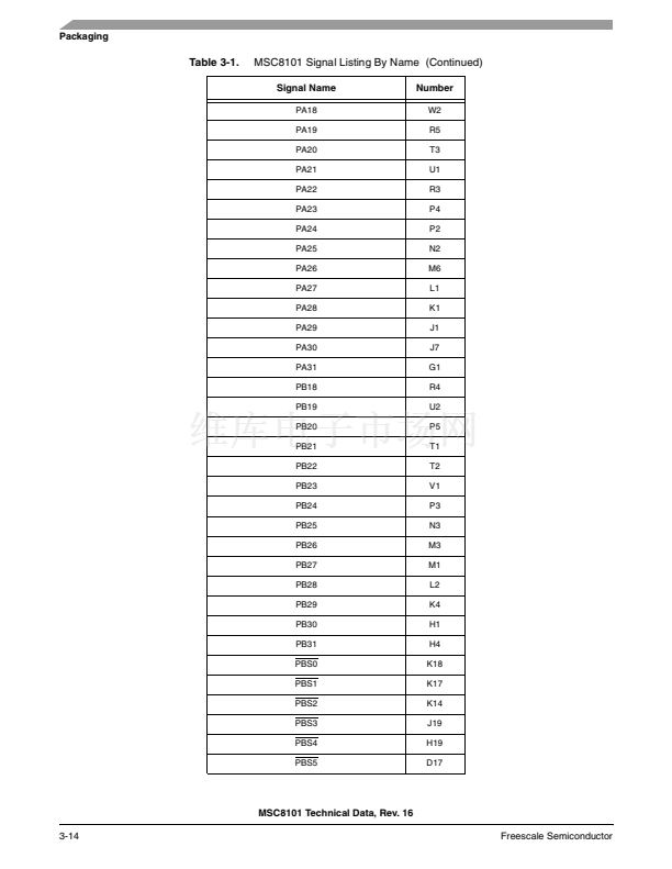
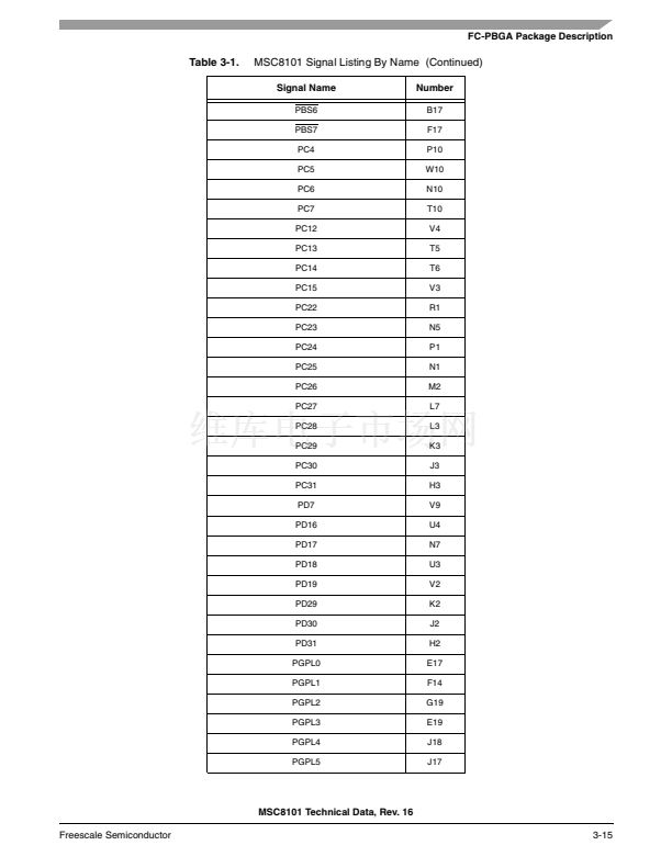
Signals/Connections
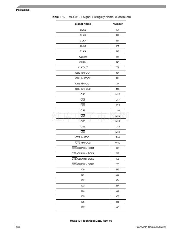
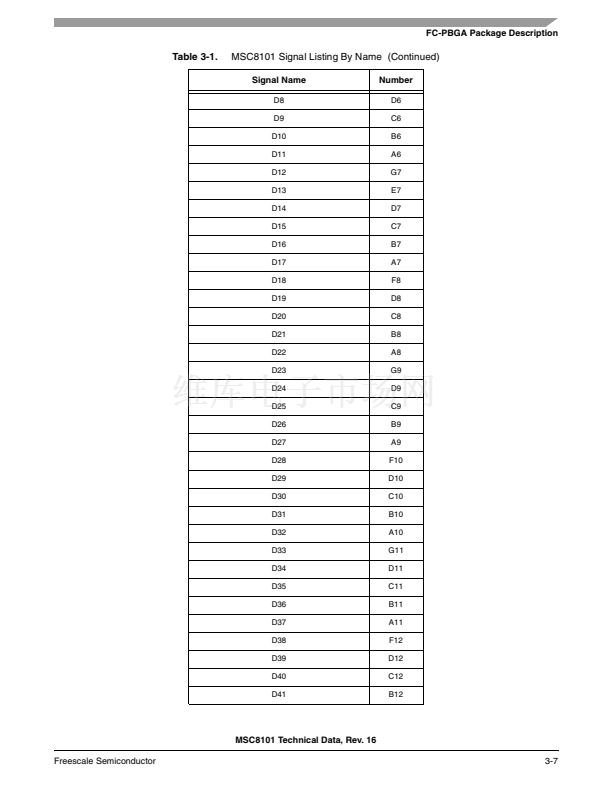
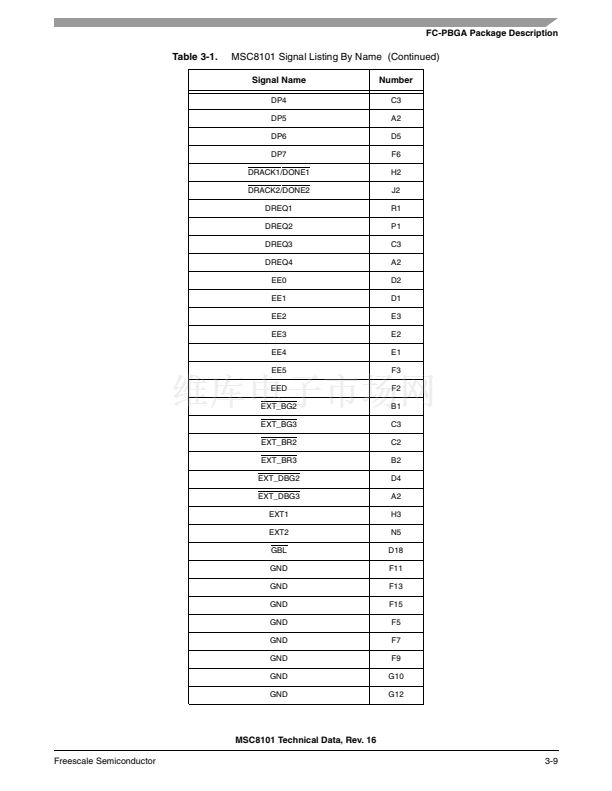
Table 1-7.
Name
General-
Purpose I/O
PA12
Port A Signals (Continued)
Peripheral Controller:
Dedicated Signal
Protocol
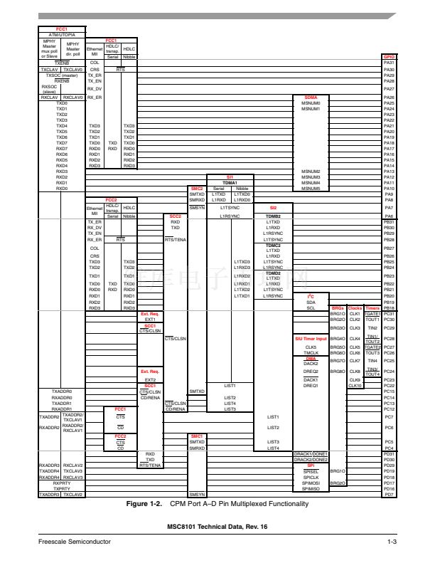
FCC1: RXD2
UTOPIA
Dedicated
I/O Data
Direction
Input
Description
FCC1: UTOPIA Receive Data Bit 2
The MSC8101 inputs ATM cell octets (UTOPIA interface data) on
RXD[0鈥?]. This is bit 2 of the receive data. RXD7 is the most significant
bit. A cell is 53 bytes. To support Multi-PHY configurations, RXD[0鈥?] is
tri-stated, enabled only when RXENB is asserted.
Module Serial Number Bit 3
The MSNUM has 6 bits that identify devices using the serial DMA
(SDMA) modules. MSNUM[0鈥?] is the sub-block code of the current
peripheral controller using SDMA. MSNUM5 indicates the section,
transmit (0) or receive (1), that is active during the transfer. The
information is recorded in the SDMA transfer error registers.
FCC1: UTOPIA RX Receive Data Bit 1
The MSC8101 inputs ATM cell octets (UTOPIA interface data) on
RXD[0鈥?]. This is bit 1 of the receive data. RXD7 is the most significant
bit. A cell is 53 bytes. To support Multi-PHY configurations, RXD[0鈥?] is
tri-stated, enabled only when RXENB is asserted.
Module Serial Number Bit 4
The MSNUM has 6 bits that identify devices using the serial DMA
(SDMA) modules. MSNUM[0鈥?] is the sub-block code of the current
peripheral controller using SDMA. MSNUM5 indicates the section,
transmit (0) or receive (1), that is active during the transfer. The
information is recorded in the SDMA transfer error registers.
FCC1: UTOPIA RX Receive Data Bit 0
The MSC8101 inputs ATM cell octets (UTOPIA interface data) on
RXD[0鈥?]. RXD0 is the least significant bit of the receive data. A cell is
53 bytes. To support Multi-PHY configurations, RXD[0鈥?] is tri-stated,
enabled only when RXENB is asserted.
Module Serial Number Bit 5
The MSNUM has 6 bits that identify devices using the serial DMA
(SDMA) modules. MSNUM[0鈥?] is the sub-block code of the current
peripheral controller using SDMA. MSNUM5 indicates the section,
transmit (0) or receive (1), that is active during the transfer. The
information is recorded in the SDMA transfer error registers.
SMC2: Serial Management Transmit Data
The SMC interface consists of SMTXD, SMRXD, SMSYN, and a clock.
Not all signals are used for all applications. SMCs are full-duplex ports
that supports three protocols or modes: UART, transparent, or general-
circuit interface (GCI). See also PC15.
Time-Division Multiplexing A1: Layer 1 Transmit Data Bit 0
L1TXD0 is the least significant bit of the TDM nibble data.
SMC2: Serial Management Receive Data
The SMC interface consists of SMTXD, SMRXD, SMSYN, and a clock.
Not all signals are used for all applications. SMCs are full-duplex ports
that supports three protocols or modes: UART, transparent, or general-
circuit interface (GCI).
Time-Division Multiplexing A1: Layer 1 Nibble Receive Data Bit 0
L1RXD0 is the least significant bit received in nibble mode.
Time-Division Multiplexing A1: Layer 1 Serial Receive Data
TDMA1 receives serial data from L1RXD.
SDMA: MSNUM3
Output
PA11
FCC1: RXD1
UTOPIA
Input
SDMA: MSNUM4
Output
PA10
FCC1: RXD0
UTOPIA
Input
SDMA: MSNUM5
Output
PA9
SMC2: SMTXD
Output
SI1 TDMA1: L1TXD0
TDM nibble
PA8
SMC2: SMRXD
Output
Input
SI1 TDMA1: L1RXD0
TDM nibble
SI1 TDMA1: L1RXD
TDM serial
Input
Input
MSC8101 Technical Data, Rev. 16
1-20
Freescale Semiconductor


 1
1
 2
2
 3
3
 4
4
 5
5
 6
6
 7
7
 8
8
 9
9
 10
10
 11
11
 12
12
 13
13
 14
14
 15
15
 16
16
 17
17
 18
18
 19
19
 20
20
 21
21
 22
22
 23
23
 24
24
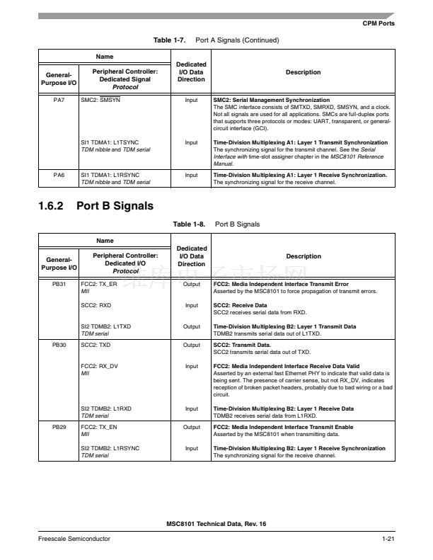 25
25
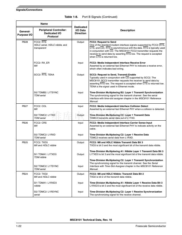 26
26
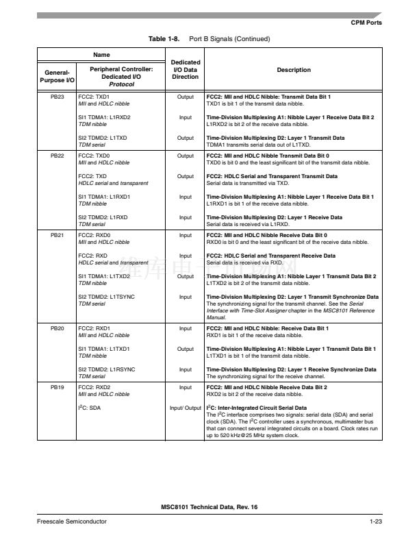 27
27
 28
28
 29
29
 30
30
 31
31
 32
32
 33
33
 34
34
 35
35
 36
36
 37
37
 38
38
 39
39
 40
40
 41
41
 42
42
 43
43
 44
44
 45
45
 46
46
 47
47
 48
48
 49
49
 50
50
 51
51
 52
52
 53
53
 54
54
 55
55
 56
56
 57
57
 58
58
 59
59
 60
60
 61
61
 62
62
 63
63
 64
64
 65
65
 66
66
 67
67
 68
68
 69
69
 70
70
 71
71
 72
72
 73
73
 74
74
 75
75
 76
76
 77
77
 78
78
 79
79
 80
80
 81
81
 82
82
 83
83
 84
84
 85
85
 86
86
 87
87
 88
88
 89
89
 90
90
 91
91
 92
92
 93
93
 94
94
 95
95
 96
96
 97
97
 98
98
 99
99
 100
100
 101
101
 102
102
 103
103
 104
104
