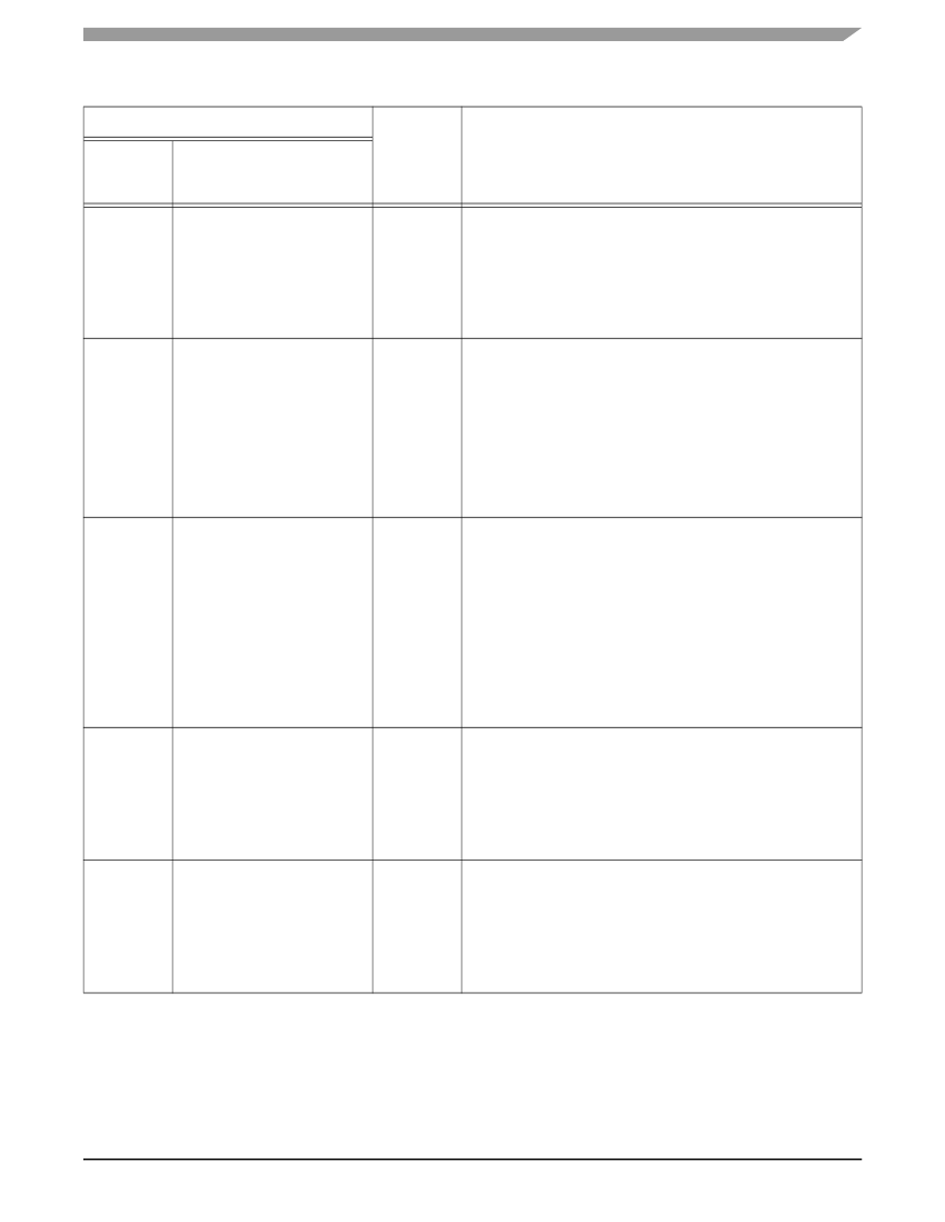
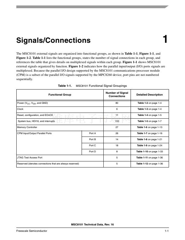
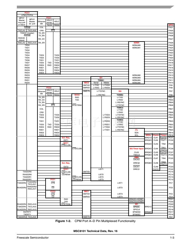
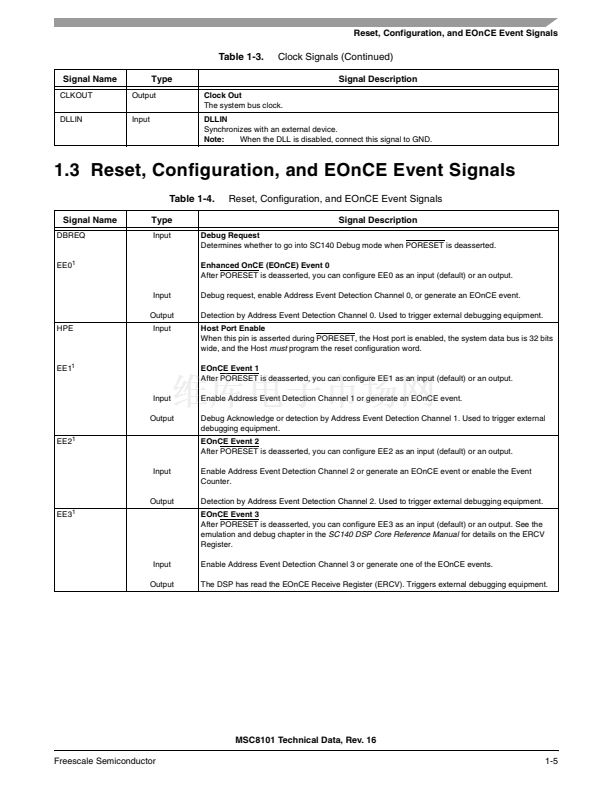
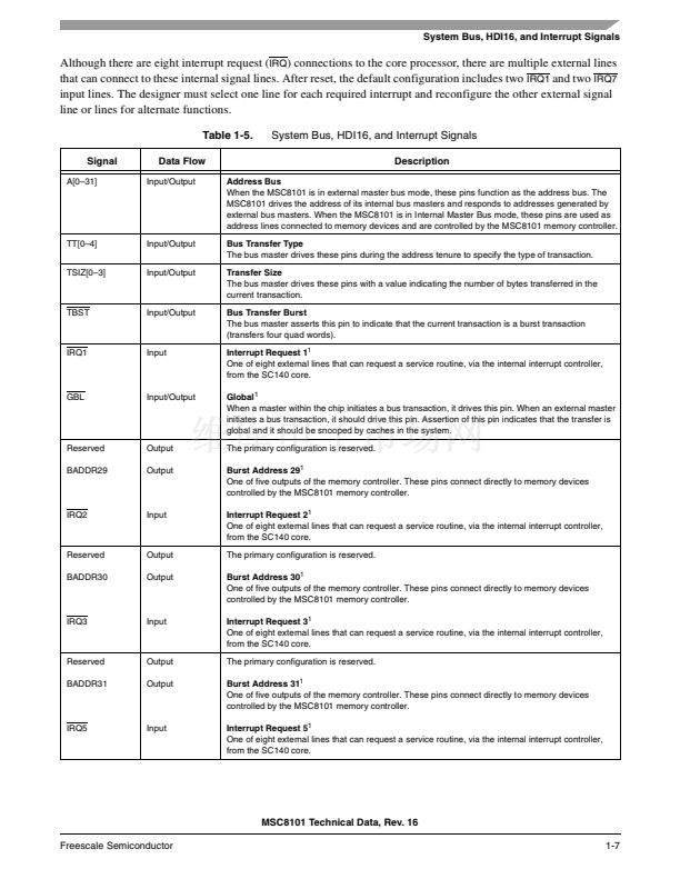
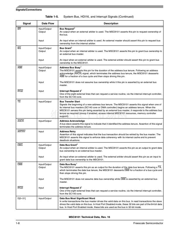
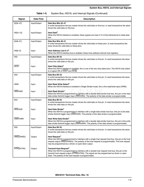
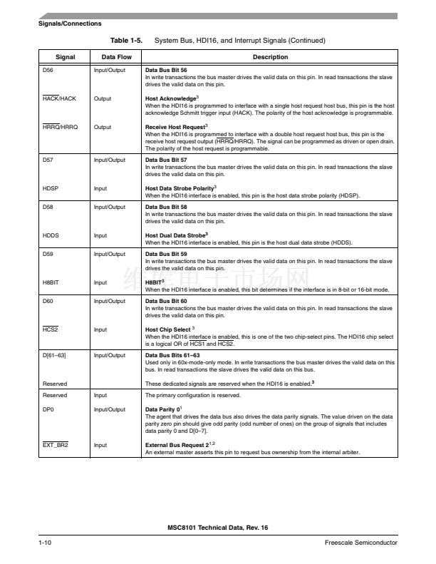
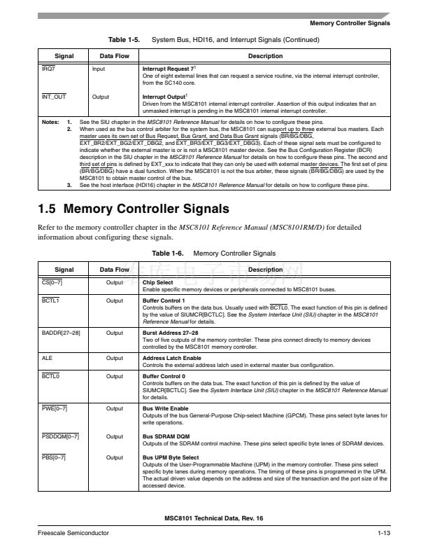
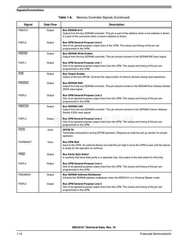
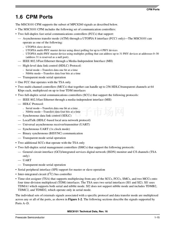
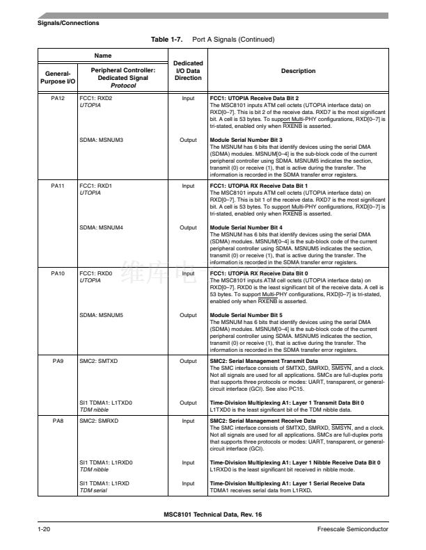
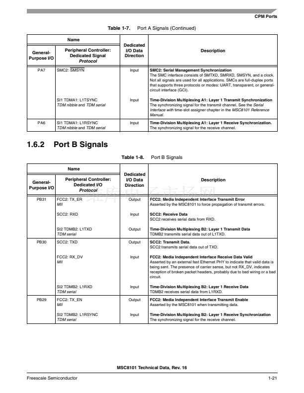
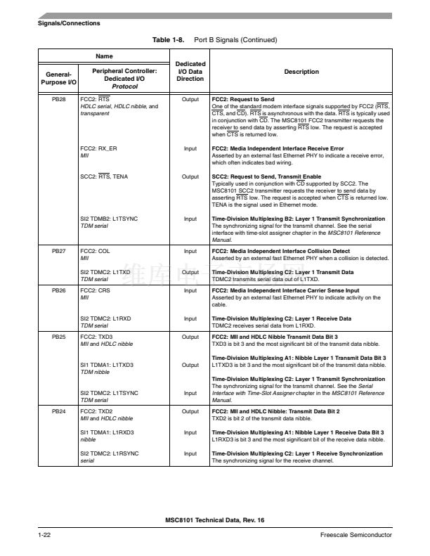
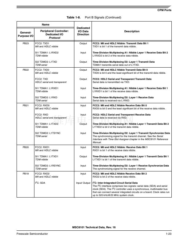
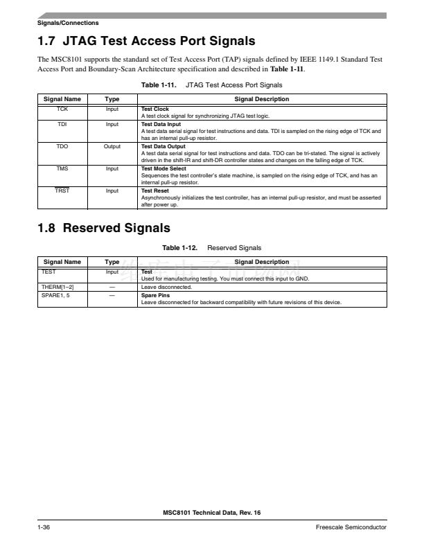
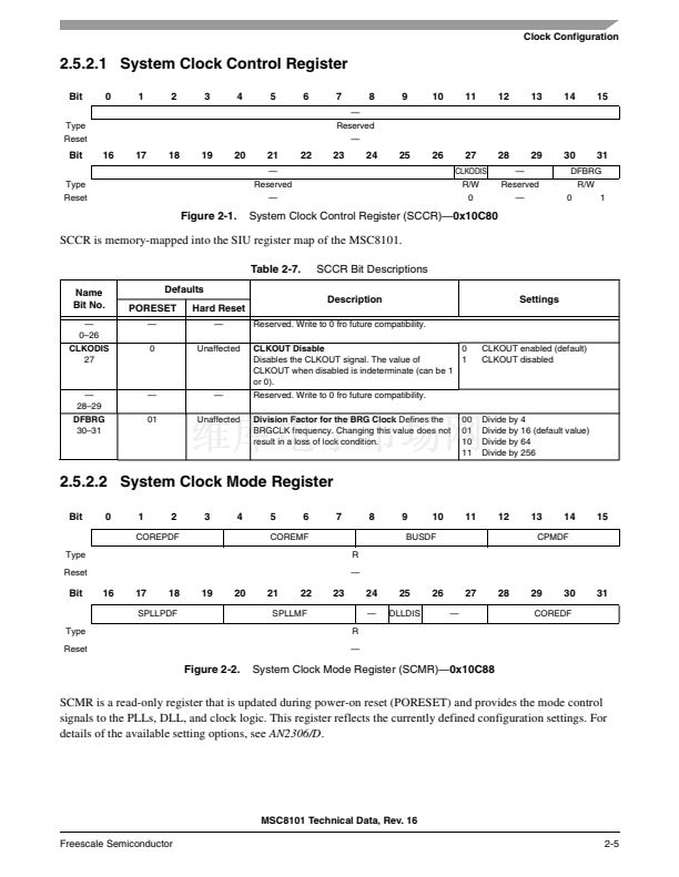
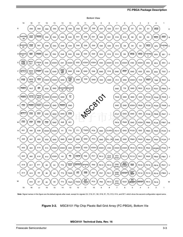
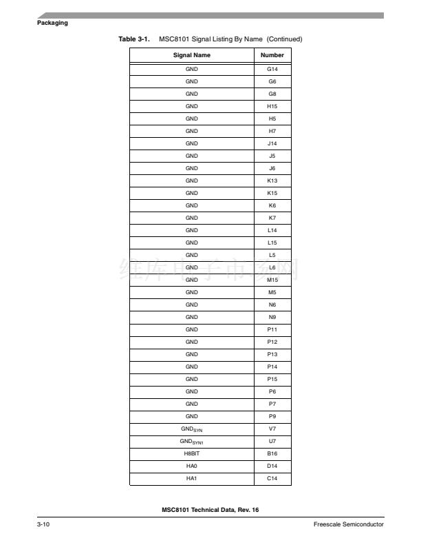
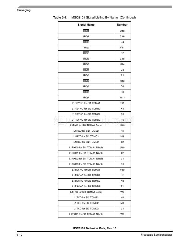
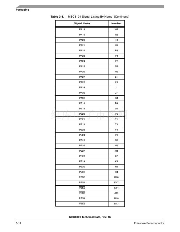
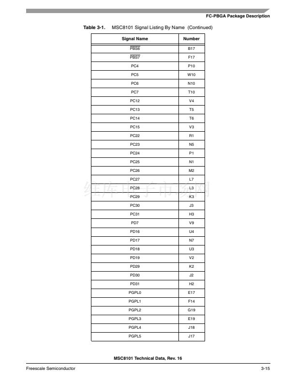
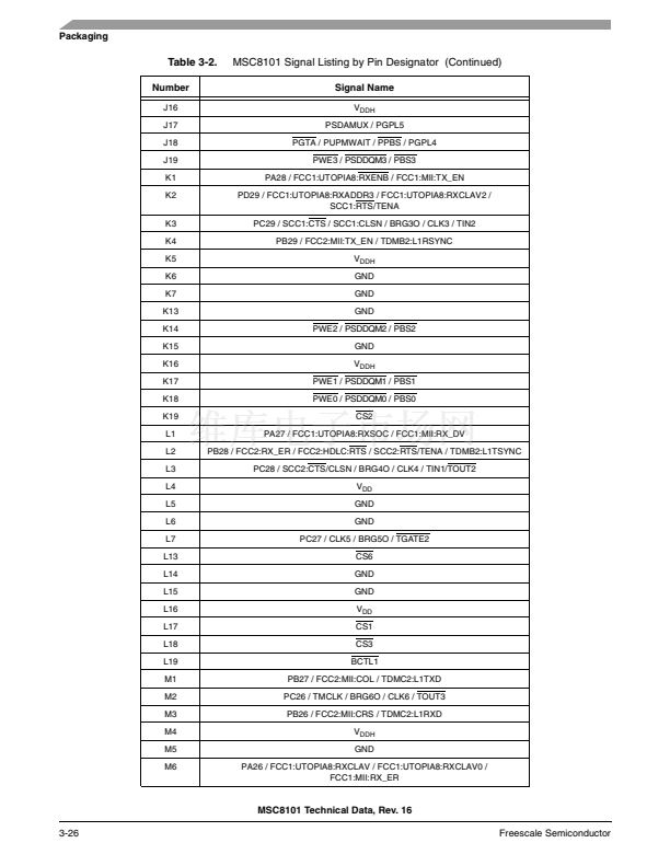
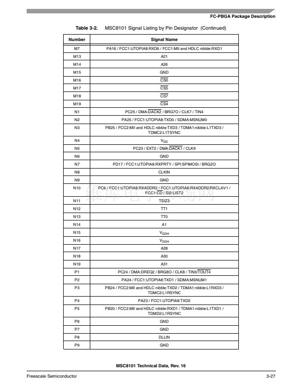
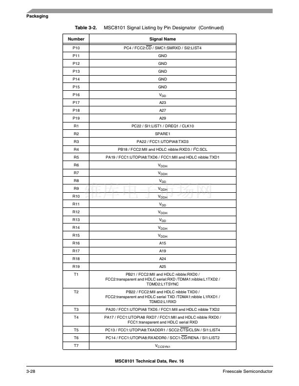
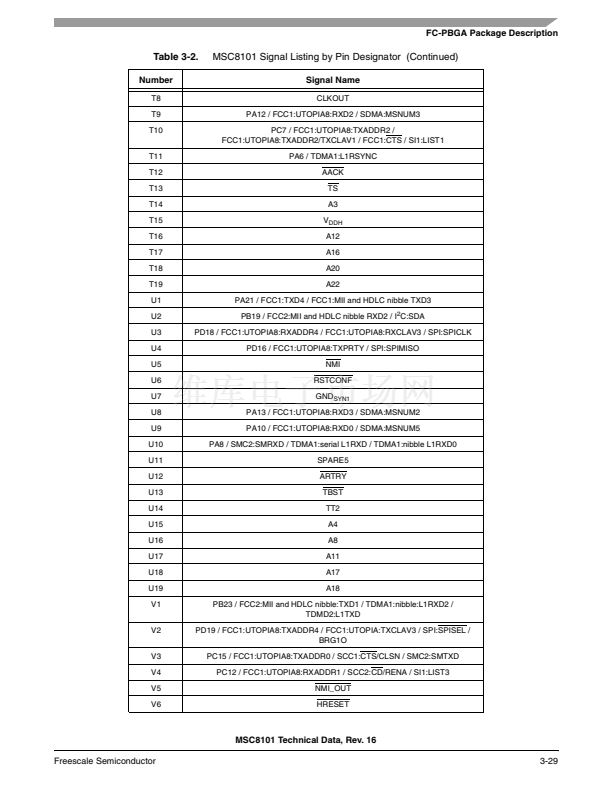
CPM Ports
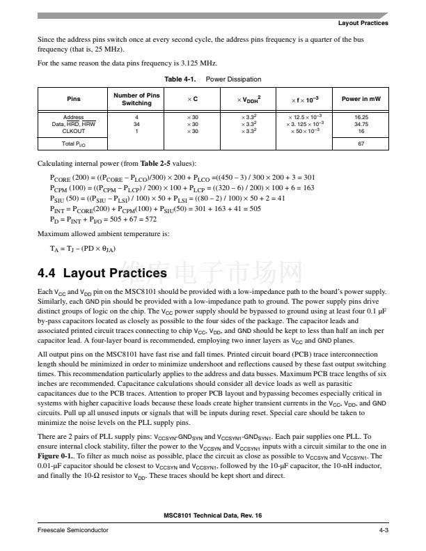
Table 1-8.
Name
General-
Purpose I/O
PB23
Port B Signals (Continued)
Peripheral Controller:
Dedicated I/O
Protocol
FCC2: TXD1
MII
and
HDLC nibble
SI1 TDMA1: L1RXD2
TDM nibble
SI2 TDMD2: L1TXD
TDM serial
Dedicated
I/O Data
Direction
Output
Description
FCC2: MII and HDLC Nibble: Transmit Data Bit 1
TXD1 is bit 1 of the transmit data nibble.
Time-Division Multiplexing A1: Nibble Layer 1 Receive Data Bit 2
L1RXD2 is bit 2 of the receive data nibble.
Time-Division Multiplexing D2: Layer 1 Transmit Data
TDMA1 transmits serial data out of L1TXD.
FCC2: MII and HDLC Nibble Transmit Data Bit 0
TXD0 is bit 0 and the least significant bit of the transmit data nibble.
FCC2: HDLC Serial and Transparent Transmit Data
Serial data is transmitted via TXD.
Time-Division Multiplexing A1: Nibble Layer 1 Receive Data Bit 1
L1RXD1 is bit 1 of the receive data nibble.
Time-Division Multiplexing D2: Layer 1 Receive Data
Serial data is received via L1RXD.
FCC2: MII and HDLC Nibble Receive Data Bit 0
RXD0 is bit 0 and the least significant bit of the receive data nibble.
FCC2: HDLC Serial and Transparent Receive Data
Serial data is received via RXD.
Time-Division Multiplexing A1: Nibble Layer 1 Transmit Data Bit 2
L1TXD2 is bit 2 of the transmit data nibble.
Time-Division Multiplexing D2: Layer 1 Transmit Synchronize Data
The synchronizing signal for the transmit channel. See the
Serial
Interface with Time-Slot Assigner
chapter in the
MSC8101 Reference
Manual.
FCC2: MII and HDLC Nibble: Receive Data Bit 1
RXD1 is bit 1 of the receive data nibble.
Time-Division Multiplexing A1: Nibble Layer 1 Transmit Data Bit 1
L1TXD1 is bit 1 of the transmit data nibble.
Time-Division Multiplexing D2: Layer 1 Receive Synchronize Data
The synchronizing signal for the receive channel.
FCC2: MII and HDLC Nibble Receive Data Bit 2
RXD2 is bit 2 of the receive data nibble.
Input
Output
Output
PB22
FCC2: TXD0
MII
and
HDLC nibble
FCC2: TXD
HDLC serial
and
transparent
SI1 TDMA1: L1RXD1
TDM nibble
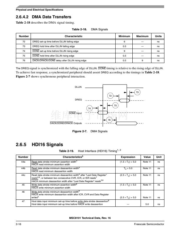
SI2 TDMD2: L1RXD
TDM serial
Output
Input
Input
Input
PB21
FCC2: RXD0
MII
and
HDLC nibble
FCC2: RXD
HDLC serial
and
transparent
SI1 TDMA1: L1TXD2
TDM nibble
SI2 TDMD2: L1TSYNC
TDM serial
Input
Output
Input
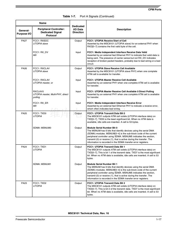
PB20
FCC2: RXD1
MII
and
HDLC nibble
SI1 TDMA1: L1TXD1
TDM nibble
SI2 TDMD2: L1RSYNC
TDM serial
Input
Output
Input
Input
PB19
FCC2: RXD2
MII
and
HDLC nibble
I
2
C: SDA
Input/ Output
I
2
C: Inter-Integrated Circuit Serial Data
The I
2
C interface comprises two signals: serial data (SDA) and serial
clock (SDA). The I
2
C controller uses a synchronous, multimaster bus
that can connect several integrated circuits on a board. Clock rates run
up to 520 kHz@25 MHz system clock.
MSC8101 Technical Data, Rev. 16
Freescale Semiconductor
1-23


 1
1
 2
2
 3
3
 4
4
 5
5
 6
6
 7
7
 8
8
 9
9
 10
10
 11
11
 12
12
 13
13
 14
14
 15
15
 16
16
 17
17
 18
18
 19
19
 20
20
 21
21
 22
22
 23
23
 24
24
 25
25
 26
26
 27
27
 28
28
 29
29
 30
30
 31
31
 32
32
 33
33
 34
34
 35
35
 36
36
 37
37
 38
38
 39
39
 40
40
 41
41
 42
42
 43
43
 44
44
 45
45
 46
46
 47
47
 48
48
 49
49
 50
50
 51
51
 52
52
 53
53
 54
54
 55
55
 56
56
 57
57
 58
58
 59
59
 60
60
 61
61
 62
62
 63
63
 64
64
 65
65
 66
66
 67
67
 68
68
 69
69
 70
70
 71
71
 72
72
 73
73
 74
74
 75
75
 76
76
 77
77
 78
78
 79
79
 80
80
 81
81
 82
82
 83
83
 84
84
 85
85
 86
86
 87
87
 88
88
 89
89
 90
90
 91
91
 92
92
 93
93
 94
94
 95
95
 96
96
 97
97
 98
98
 99
99
 100
100
 101
101
 102
102
 103
103
 104
104
