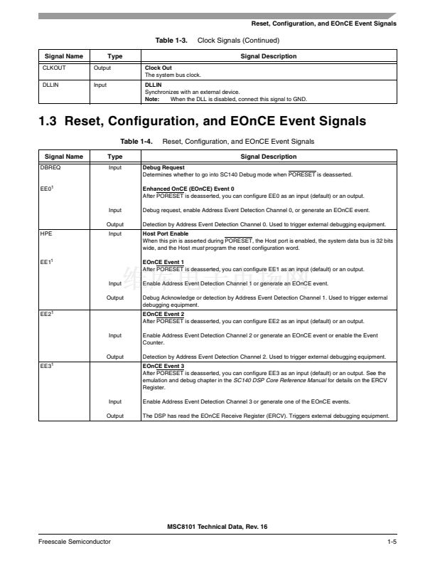
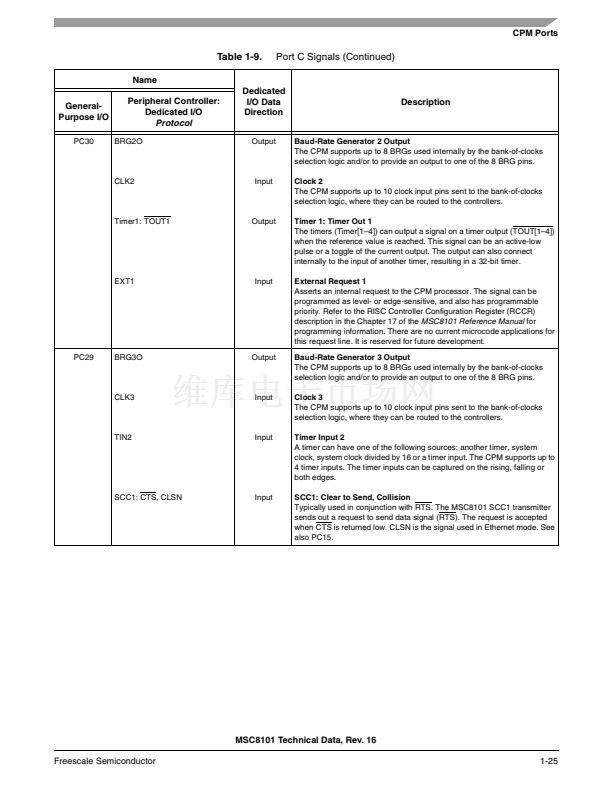
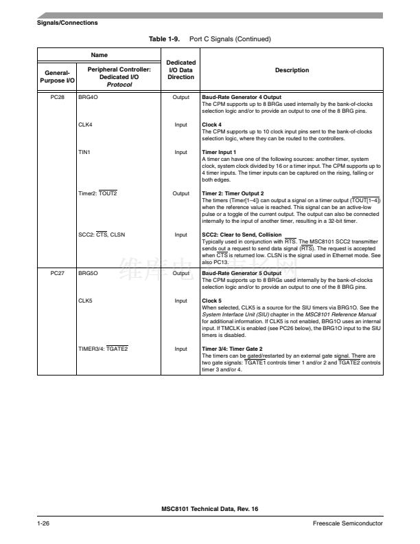
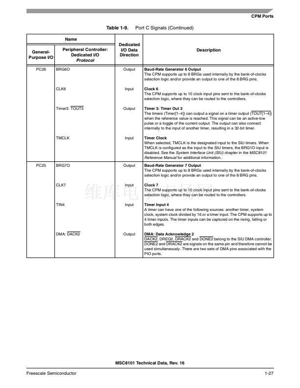
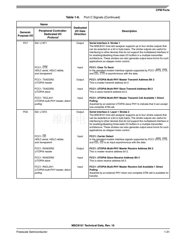
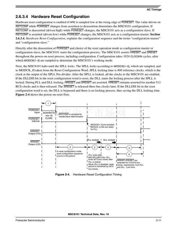
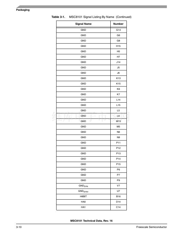
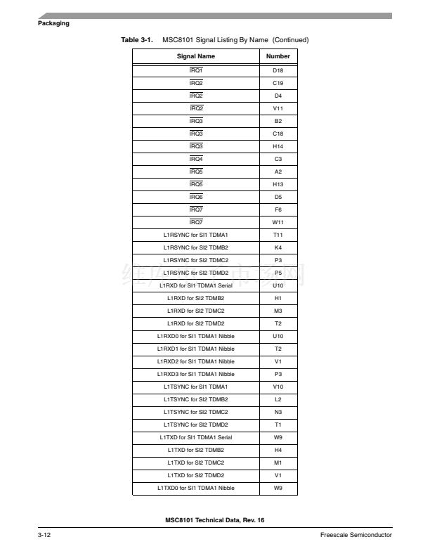
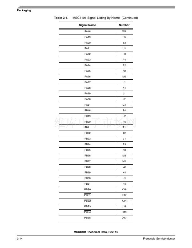
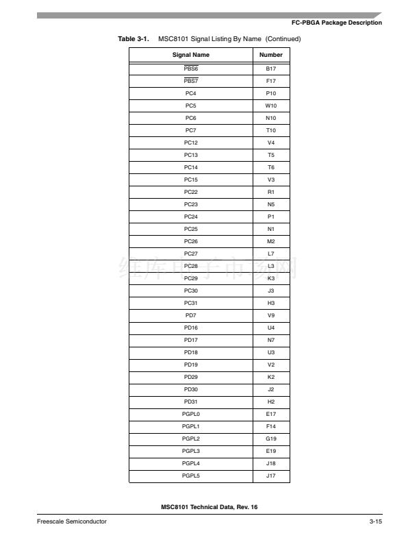
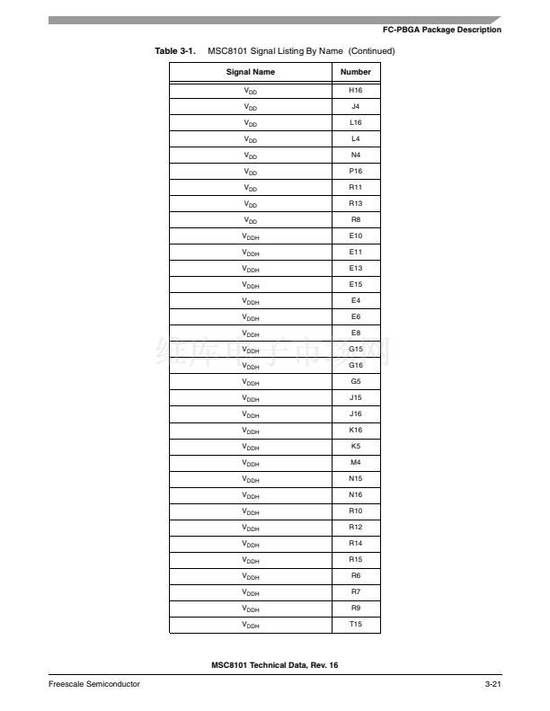
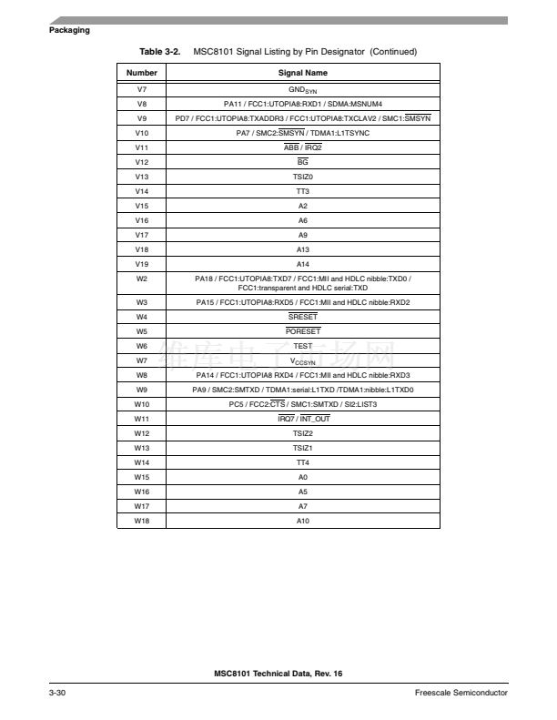
AC Timings
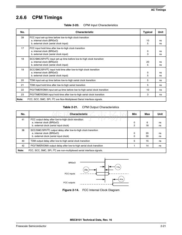
DLLIN
23
22
PIO/TIMER/DMA inputs
42
PIO/TIMER/DMA outputs
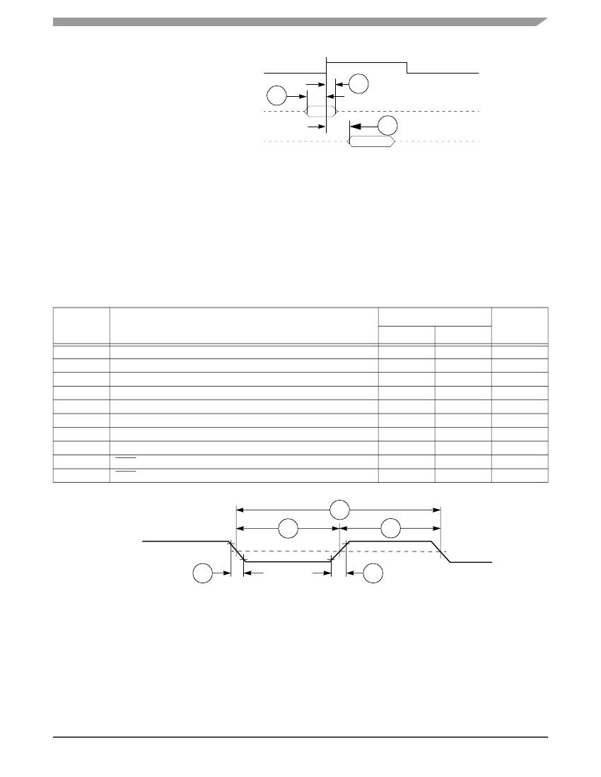
Figure 2-19.
PIO, Timer, and DMA Signal Diagram
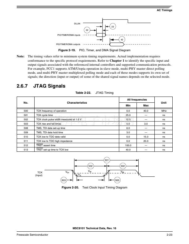
Note:
The timing values refer to minimum system timing requirements. Actual implementation requires
conformance to the specific protocol requirements. Refer to
Chapter 1
to identify the specific input and
output signals associated with the referenced internal controllers and supported communication protocols.
For example, FCC1 supports ATM/Utopia operation in slave mode, multi-PHY master direct polling
mode, and multi-PHY master multiplexed polling mode and each of these modes supports its own set of
signals; the direction (input or output) of some of the shared signal names depends on the selected mode.
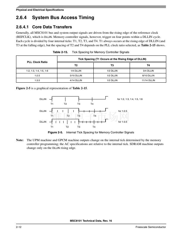
2.6.7
JTAG Signals
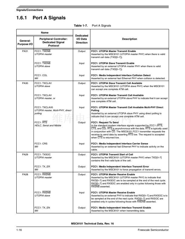
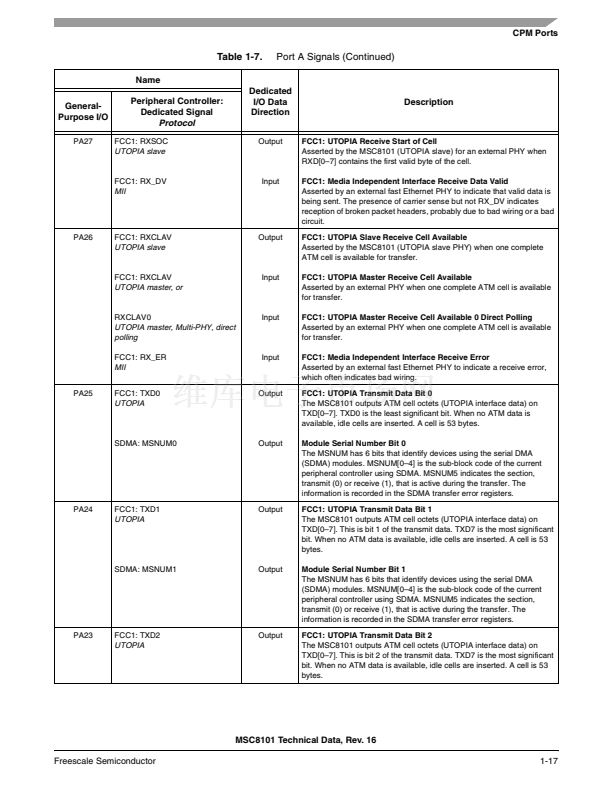
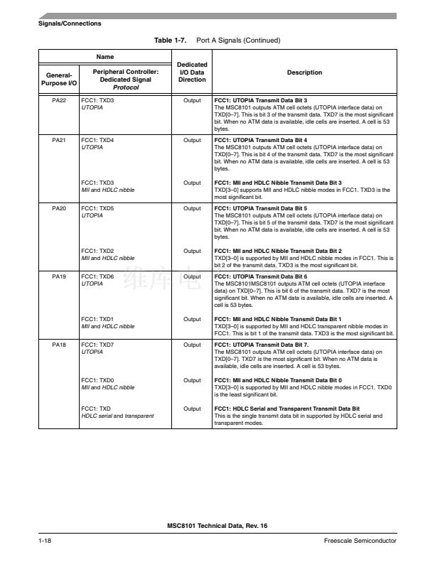
Table 2-22.
JTAG Timing
All frequencies
Unit
Min
Max
40.0
鈥?/div>
鈥?/div>
3.0
鈥?/div>
鈥?/div>
15.0
20.0
鈥?/div>
鈥?/div>
MHz
ns
ns
ns
ns
ns
ns
ns
ns
ns
0.0
25.0
12.5
0.0
6.0
3.0
0.0
0.0
100.0
40.0
No.
500
501
502
503
508
509
510
511
512
513
TCK frequency of operation
TCK cycle time
Characteristics
TCK clock pulse width measured at 1.6 V
TCK rise and fall times
TMS, TDI data set-up time
TMS, TDI data hold time
TCK low to TDO data valid
TCK low to TDO high impedance
TRST assert time
TRST set-up time to TCK low
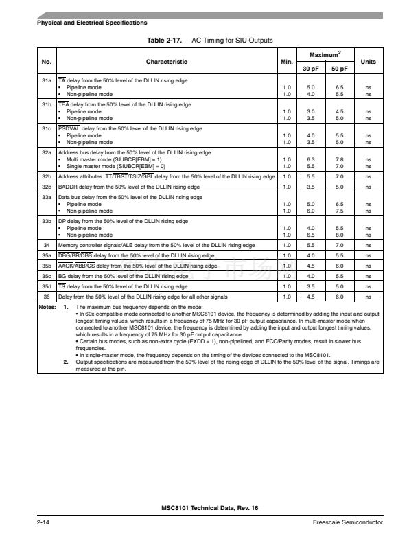
501
502
TCK
(Input)
V
IH
503
V
M
V
IL
503
502
V
M
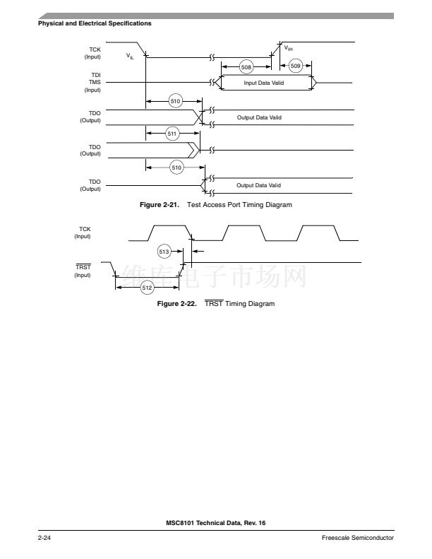
Figure 2-20.
Test Clock Input Timing Diagram
MSC8101 Technical Data, Rev. 16
Freescale Semiconductor
2-23
MSC8101 PDF文件相关型号
MSC8101D
MSC8101相关型号PDF文件下载
-
型号
版本
描述
厂商
下载
-
英文版
Advanced Semiconductor [HIGH POWER GaAs FET]
ASI
-
英文版
Advanced Semiconductor [HIGH POWER GaAs FET]
ASI
-
英文版
Silicon Errata for the MSC8101 Processor, Mask 0K40A
FREESCALE
-
英文版
Networking Digital Signal Processor
-
英文版
MSC8102 Technical Data
-
英文版
Network-Ready DSP
-
英文版
MSC8112 Data Sheet
-
英文版
MSC8113 Data Sheet
-
英文版
MSC8122 Technical Data Sheeet
-
英文版
MSC8126 Technical Data Sheet
-
英文版
MSC8144 Quad Core Digital Signal Processor Data Sheet
-
英文版
MSC8151 Data Sheet
-
英文版
MSC8152 Data Sheet
-
英文版
MSC8154 Data Sheet
-
英文版
MSC8156 Data Sheet
-
英文版
Advanced Power Technology [RF & MICROWAVE TRANSISTORS G...
ADPOW
-
英文版
NPN RF TRANSISTOR
ASI
-
英文版
NPN RF TRANSISTOR
ASI [Advan...
-
英文版
RF & MICROWAVE TRANSISTORS GENERAL PURPOSE LINEAR APPLICATIO...
-
英文版
RF & MICROWAVE TRANSISTORS GENERAL PURPOSE LINEAR APPLICATIO...
STMICROELECTRON...


 1
1
 2
2
 3
3
 4
4
 5
5
 6
6
 7
7
 8
8
 9
9
 10
10
 11
11
 12
12
 13
13
 14
14
 15
15
 16
16
 17
17
 18
18
 19
19
 20
20
 21
21
 22
22
 23
23
 24
24
 25
25
 26
26
 27
27
 28
28
 29
29
 30
30
 31
31
 32
32
 33
33
 34
34
 35
35
 36
36
 37
37
 38
38
 39
39
 40
40
 41
41
 42
42
 43
43
 44
44
 45
45
 46
46
 47
47
 48
48
 49
49
 50
50
 51
51
 52
52
 53
53
 54
54
 55
55
 56
56
 57
57
 58
58
 59
59
 60
60
 61
61
 62
62
 63
63
 64
64
 65
65
 66
66
 67
67
 68
68
 69
69
 70
70
 71
71
 72
72
 73
73
 74
74
 75
75
 76
76
 77
77
 78
78
 79
79
 80
80
 81
81
 82
82
 83
83
 84
84
 85
85
 86
86
 87
87
 88
88
 89
89
 90
90
 91
91
 92
92
 93
93
 94
94
 95
95
 96
96
 97
97
 98
98
 99
99
 100
100
 101
101
 102
102
 103
103
 104
104
