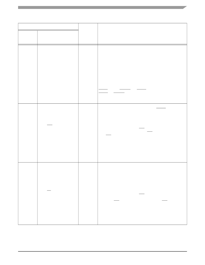
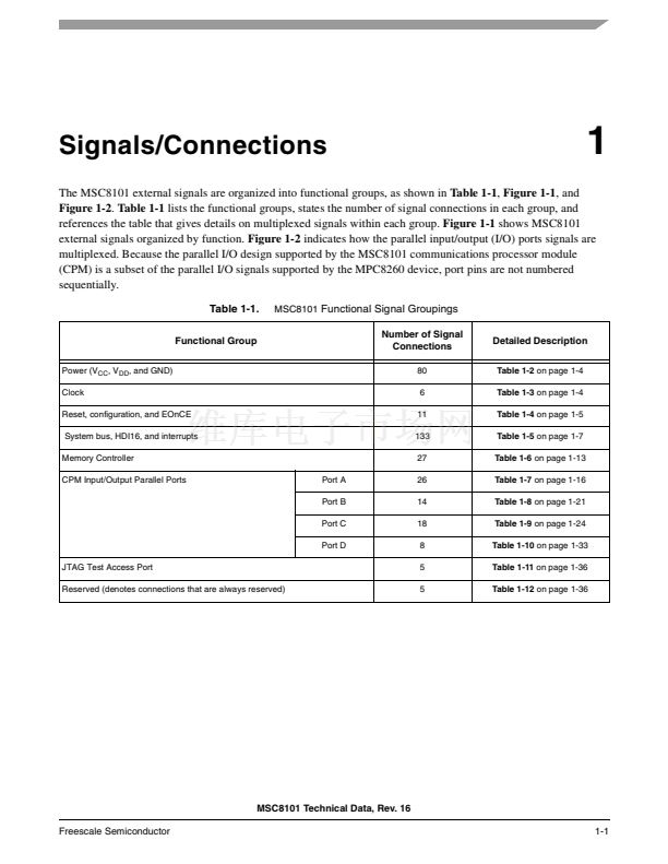
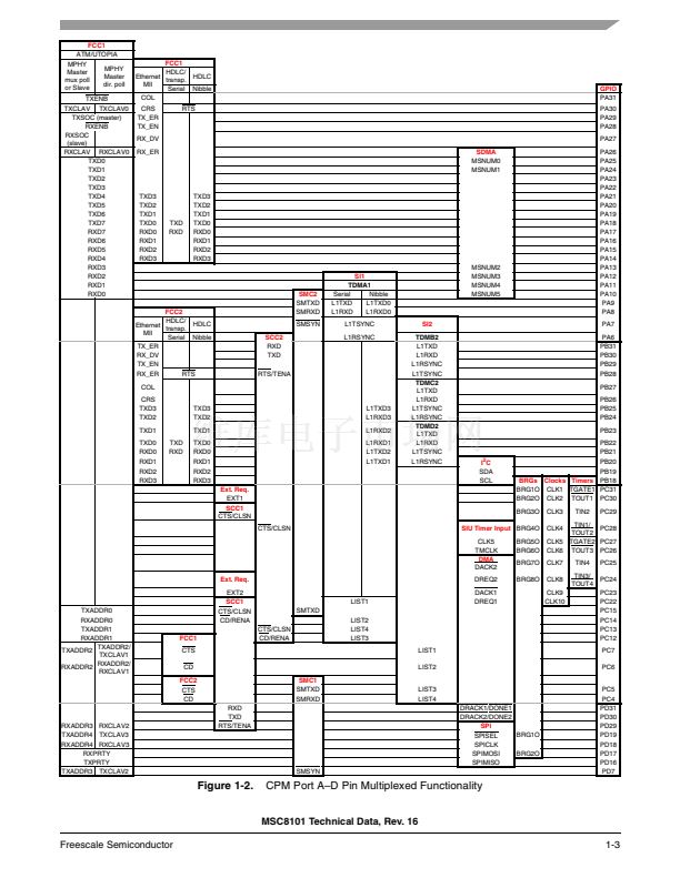
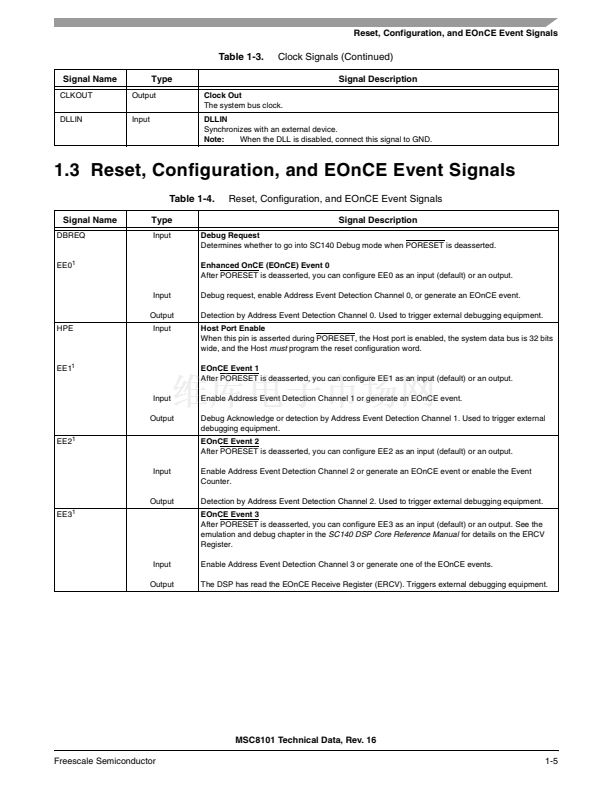
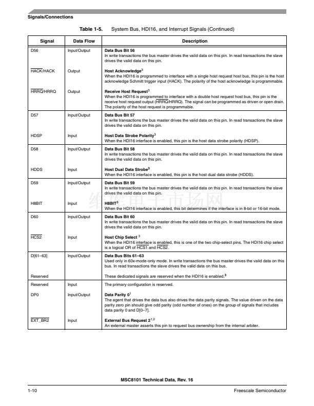
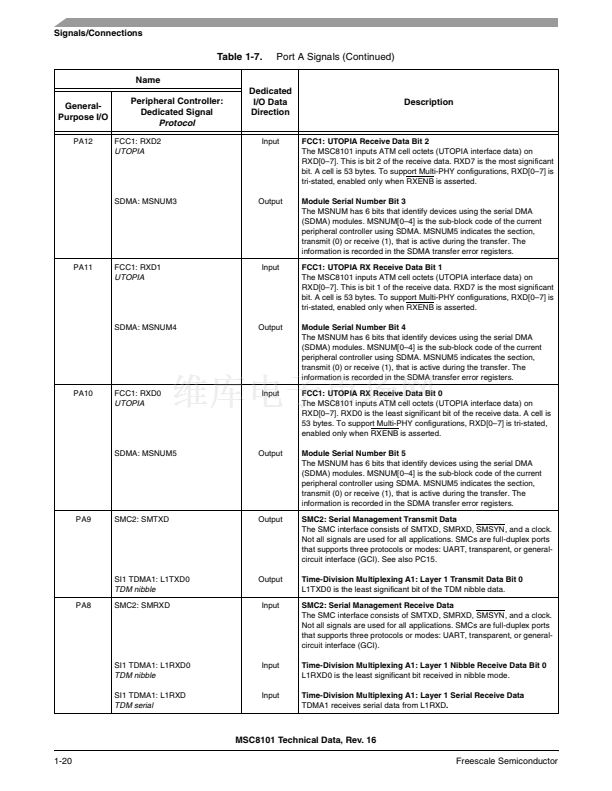
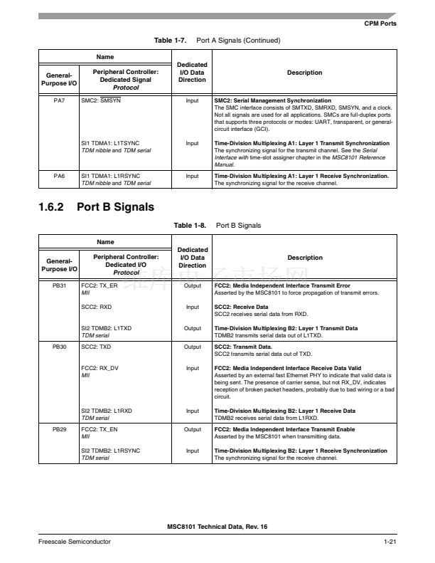
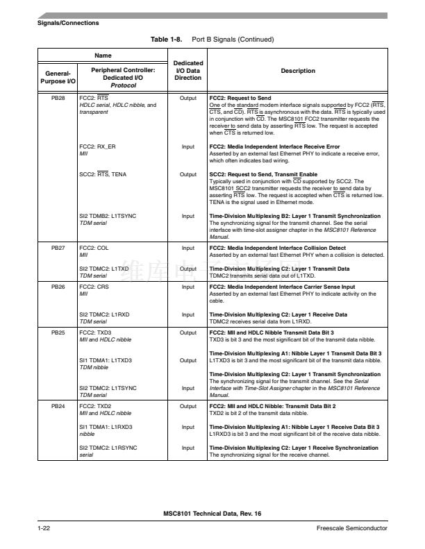
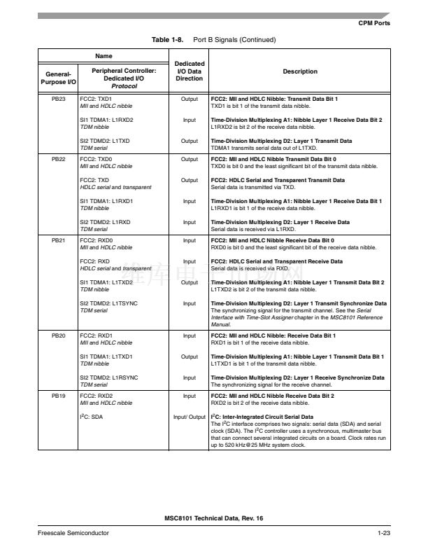
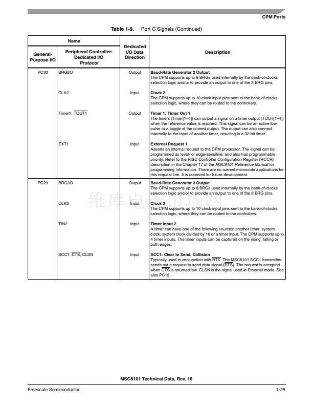
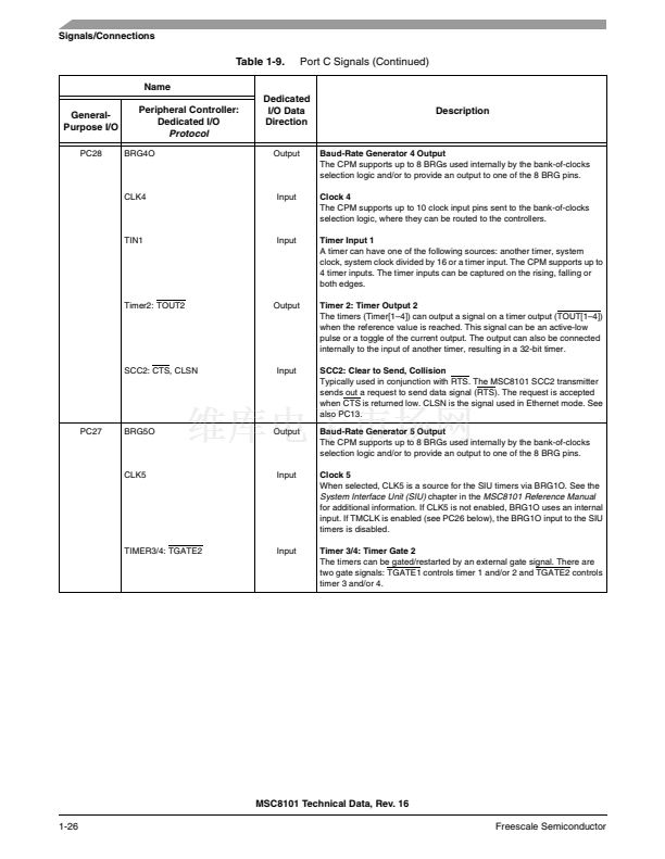
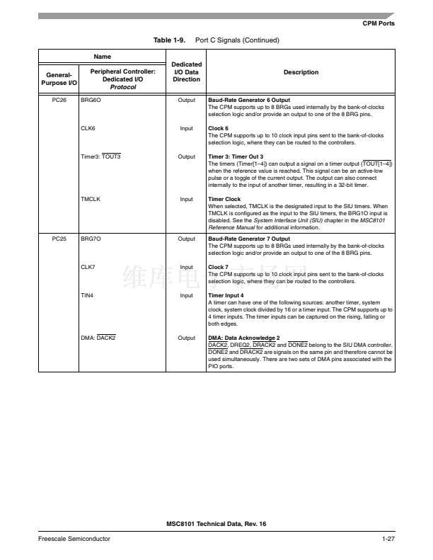
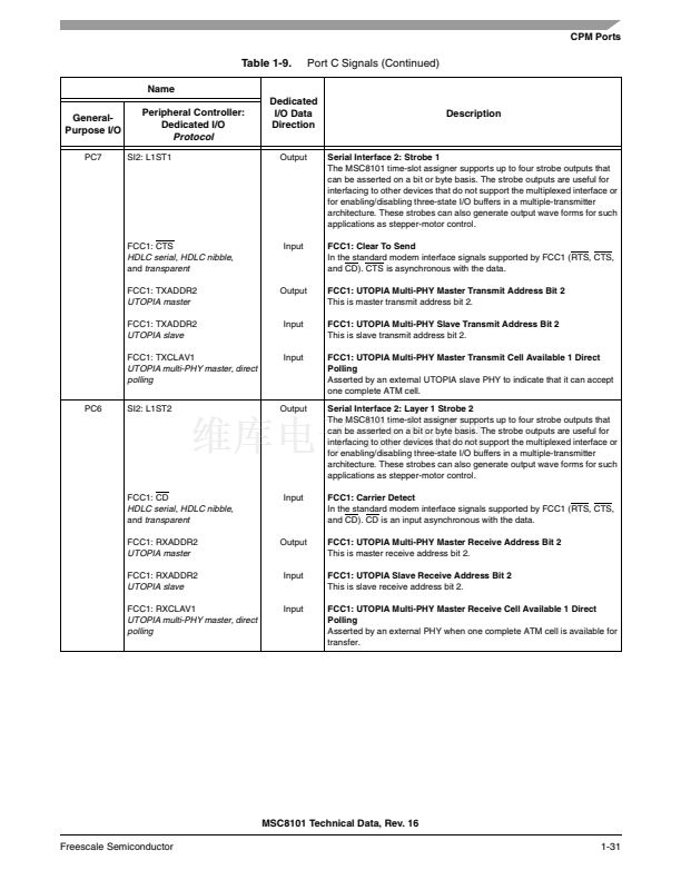
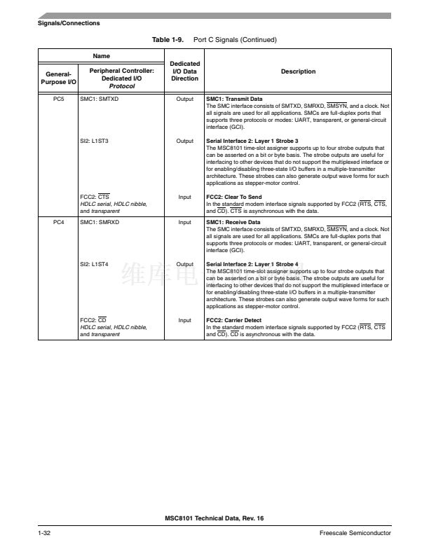
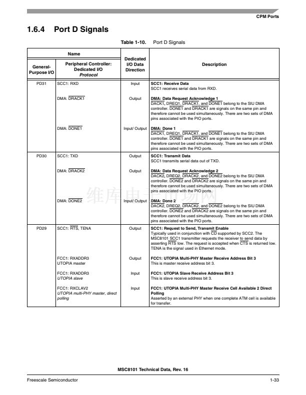
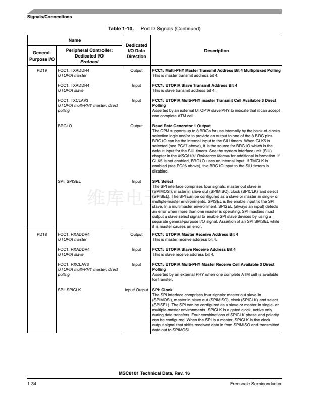
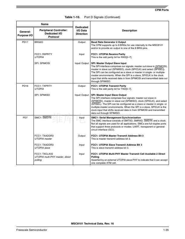
CPM Ports
Table 1-9.
Name
General-
Purpose I/O
PC22
Port C Signals (Continued)
Peripheral Controller:
Dedicated I/O
Protocol
SI1: L1ST1
Dedicated
I/O Data
Direction
Output
Description
Serial Interface 1: Layer 1 Strobe 1
The MSC8101 time-slot assigner supports up to four strobe outputs that
can be asserted on a bit or byte basis. The strobe outputs are useful for
interfacing to other devices that do not support the multiplexed interface or
for enabling/disabling three-state I/O buffers in a multiple-transmitter
architecture. These strobes can also generate output wave forms for such
applications as stepper-motor control.
Clock 10
The CPM supports up to 10 clock input pins sent to the bank-of-clocks
selection logic, where they can be routed to the controllers.
CLK10
Input
DMA: DREQ1
Input/ Output
DMA: Request 1
DACK1, DREQ1, DRACK1, and DONE1 belong to the SIU DMA controller.
DONE1 and DRACK1 are signals on the same pin and therefore cannot be
used simultaneously. There are two sets of DMA pins associated with the
PIO ports.
Output
SMC2: Serial Management Transmit Data
The SMC interface consists of SMTXD, SMRXD, SMSYN, and a clock. Not
all signals are used for all applications. SMCs are full-duplex ports that
support three protocols or modes: UART, transparent, or general-circuit
interface (GCI). See also PA9.
SCC1: Clear To Send, Collision
Typically used in conjunction with RTS. The MSC8101 SCC1 transmitter
sends out a request to send data signal (RTS). The request is accepted
when CTS is returned low. CLSN is the signal used in Ethernet mode. See
also PC29.
FCC1: UTOPIA Master Transmit Address Bit 0
This is master transmit address bit 0.
FCC1: UTOPIA Slave Transmit Address Bit 0
This is slave transmit address bit 0.
Serial Interface 1: Layer 1 Strobe 2
The MSC8101 time-slot assigner supports up to four strobe outputs that
can be asserted on a bit or byte basis. The strobe outputs are useful for
interfacing to other devices that do not support the multiplexed interface or
for enabling/disabling three-state I/O buffers in a multiple-transmitter
architecture. These strobes can also be generate output wave forms for
such applications as stepper-motor control.
SCC1: Carrier Detect, Receive Enable
Typically used in conjunction with RTS supported by SCC1. The
MSC8101MSC8101 SCC1 transmitter requests the receiver to send data
by asserting RTS low. The request is accepted when CTS is returned low.
FCC1: UTOPIA Multi-PHY Master Receive Address Bit 0
This is master receive address bit 0.
FCC1: UTOPIA Multi-PHY Slave Receive Address Bit 0
This is slave receive address bit 0.
PC15
SMC2: SMTXD
SCC1: CTS/CLSN
Input
FCC1: TXADDR0
UTOPIA master
FCC1: TXADDR0
UTOPIA slave
PC14
SI1: L1ST2
Output
Input
Output
SCC1: CD, RENA
Input
FCC1: RXADDR0
UTOPIA master
FCC1: RXADDR0
UTOPIA slave
Output
Input
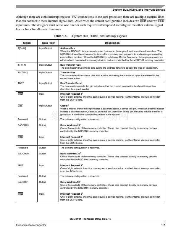
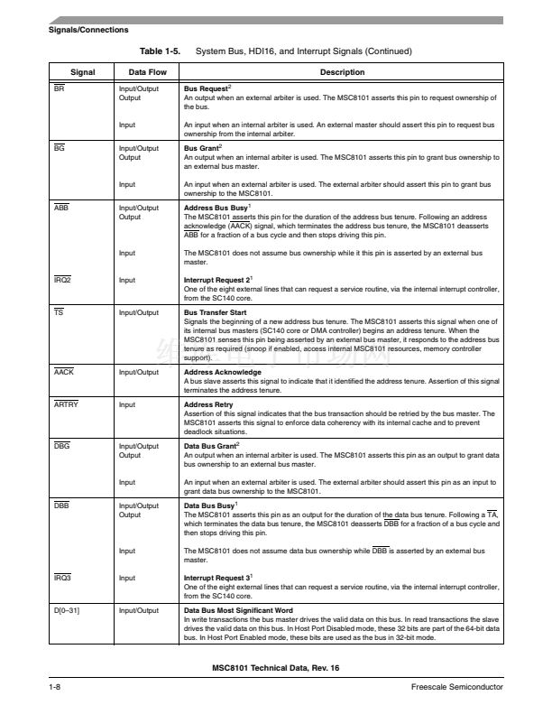
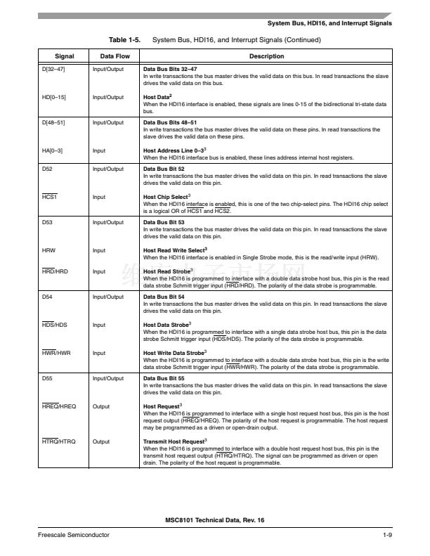
MSC8101 Technical Data, Rev. 16
Freescale Semiconductor
1-29


 1
1
 2
2
 3
3
 4
4
 5
5
 6
6
 7
7
 8
8
 9
9
 10
10
 11
11
 12
12
 13
13
 14
14
 15
15
 16
16
 17
17
 18
18
 19
19
 20
20
 21
21
 22
22
 23
23
 24
24
 25
25
 26
26
 27
27
 28
28
 29
29
 30
30
 31
31
 32
32
 33
33
 34
34
 35
35
 36
36
 37
37
 38
38
 39
39
 40
40
 41
41
 42
42
 43
43
 44
44
 45
45
 46
46
 47
47
 48
48
 49
49
 50
50
 51
51
 52
52
 53
53
 54
54
 55
55
 56
56
 57
57
 58
58
 59
59
 60
60
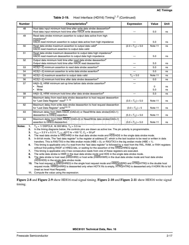
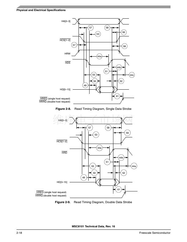
 61
61
 62
62
 63
63
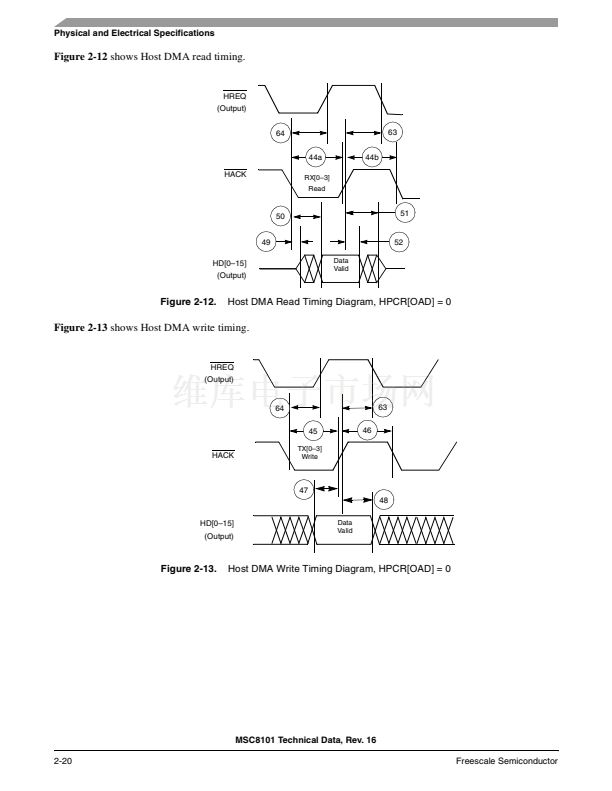
 64
64
 65
65
 66
66
 67
67
 68
68
 69
69
 70
70
 71
71
 72
72
 73
73
 74
74
 75
75
 76
76
 77
77
 78
78
 79
79
 80
80
 81
81
 82
82
 83
83
 84
84
 85
85
 86
86
 87
87
 88
88
 89
89
 90
90
 91
91
 92
92
 93
93
 94
94
 95
95
 96
96
 97
97
 98
98
 99
99
 100
100
 101
101
 102
102
 103
103
 104
104
