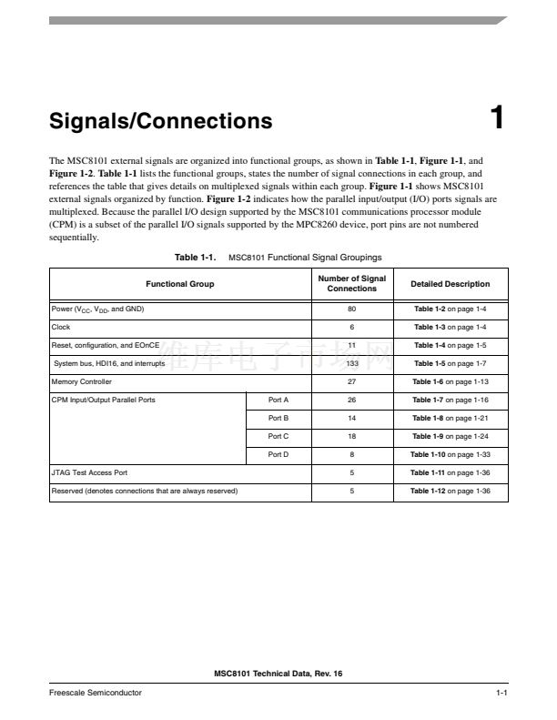
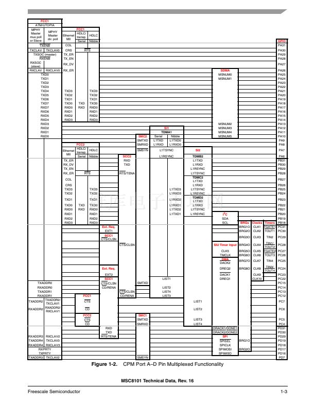
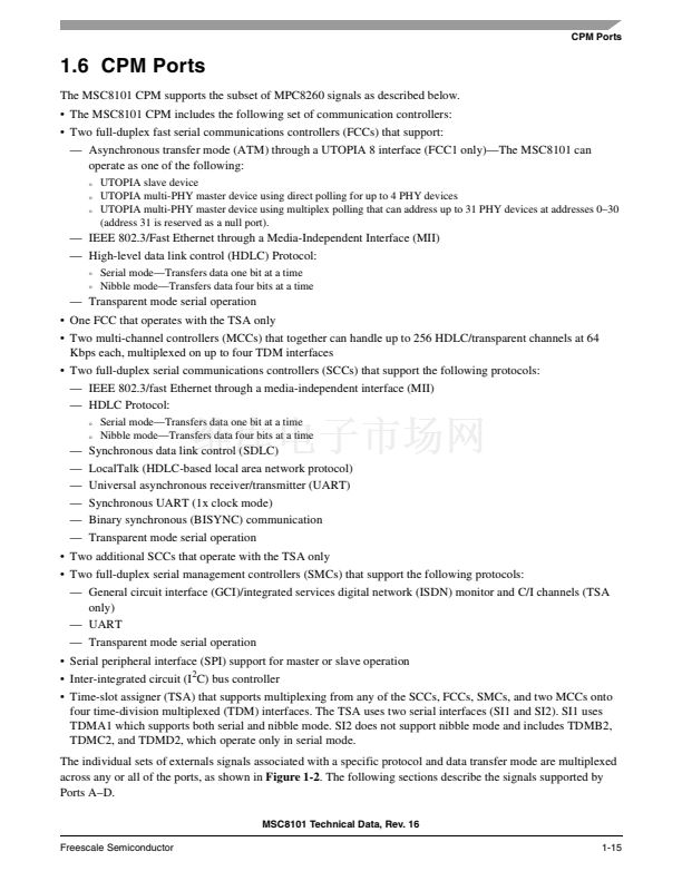
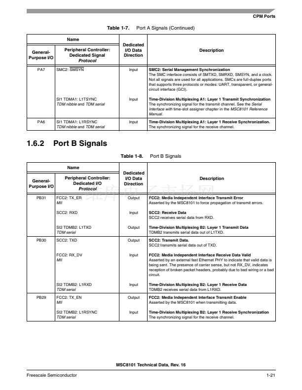
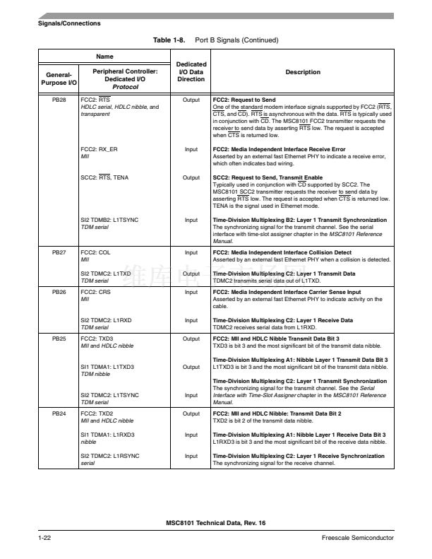
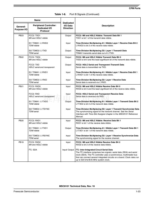
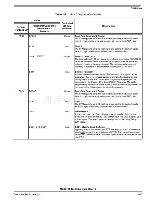
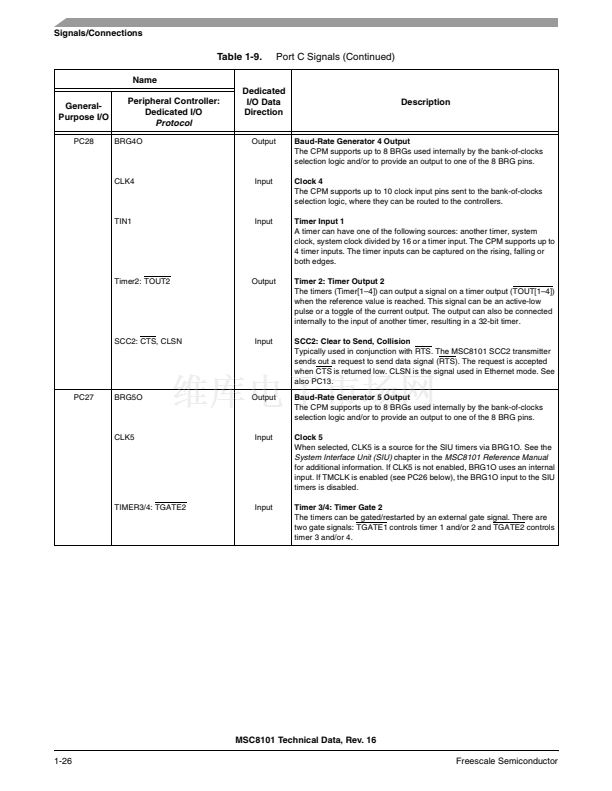
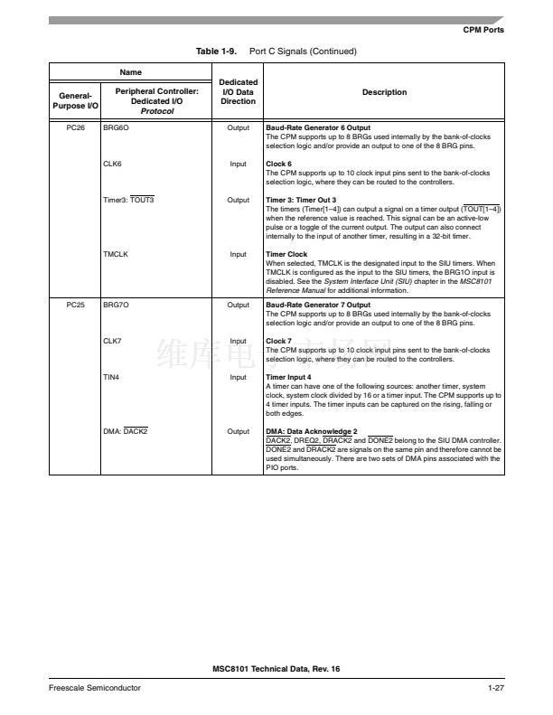
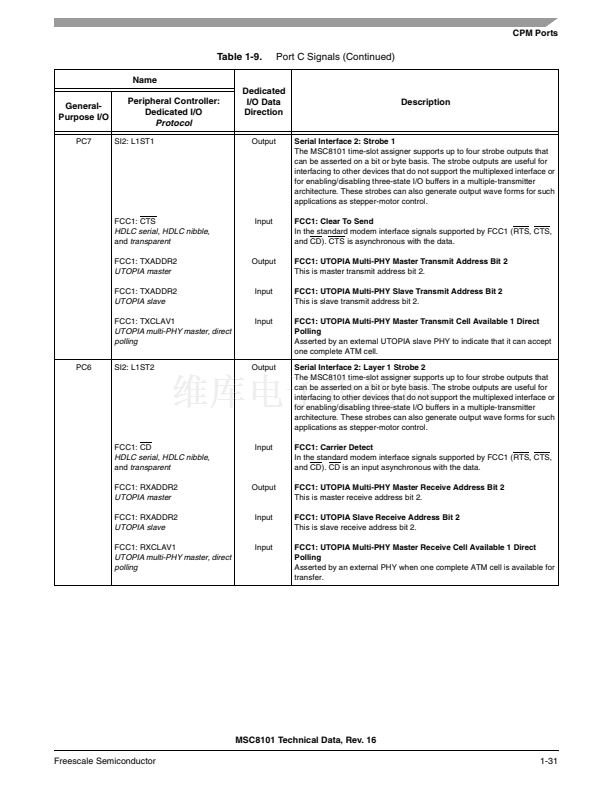
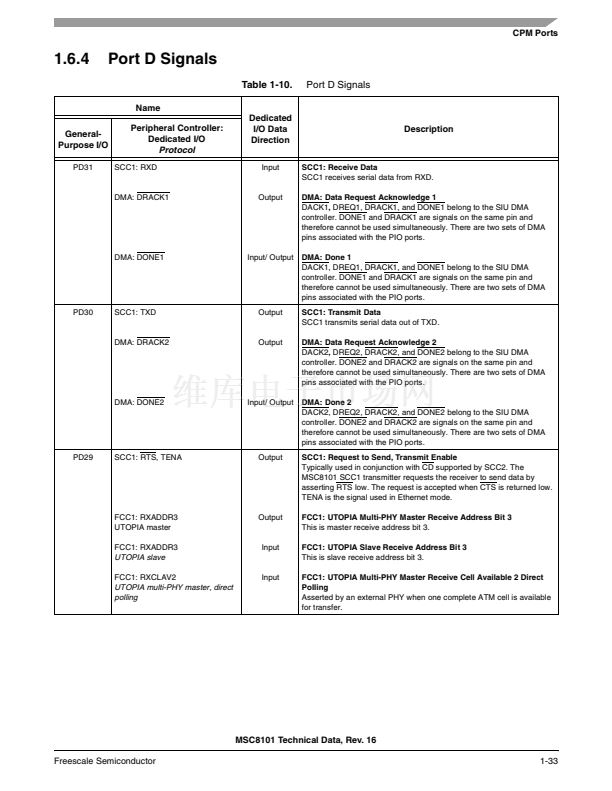
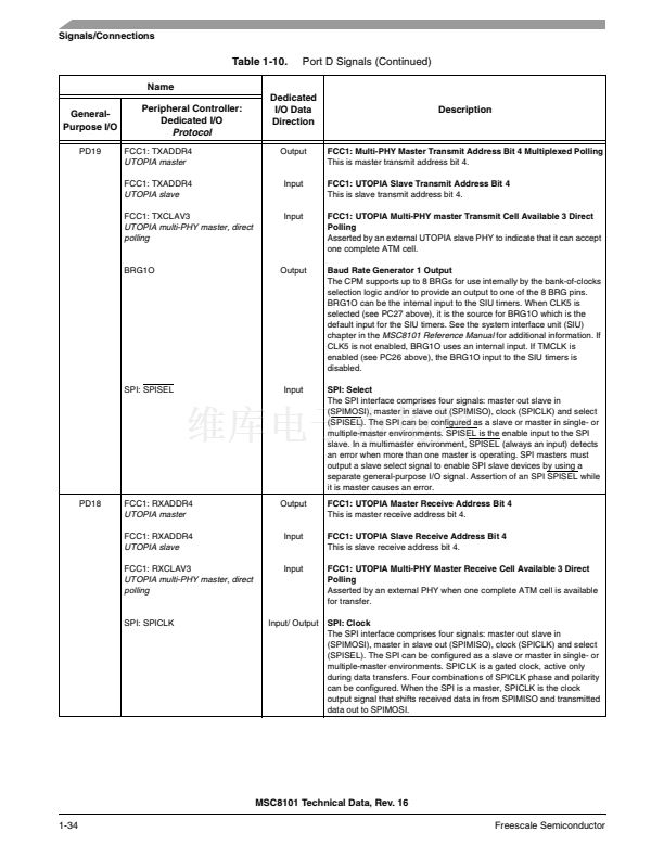
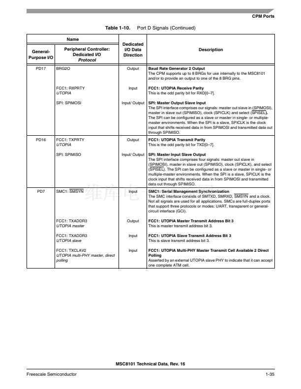
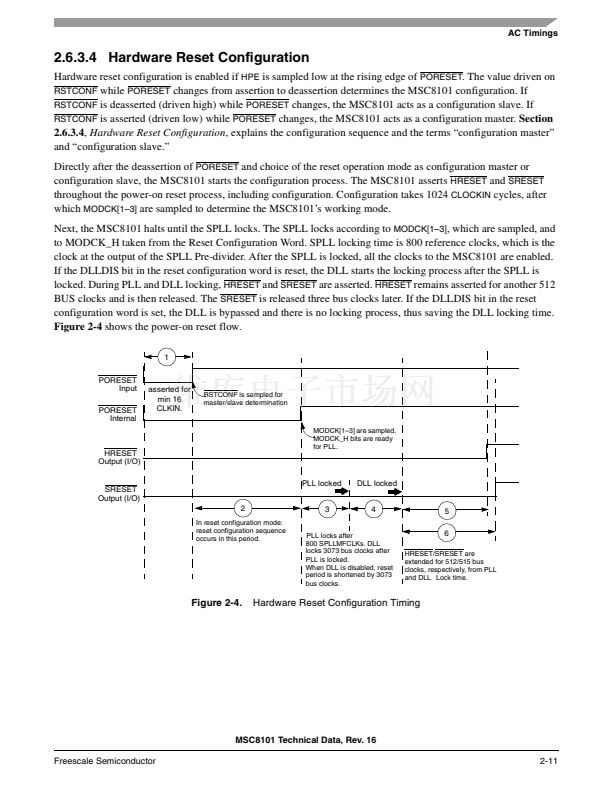
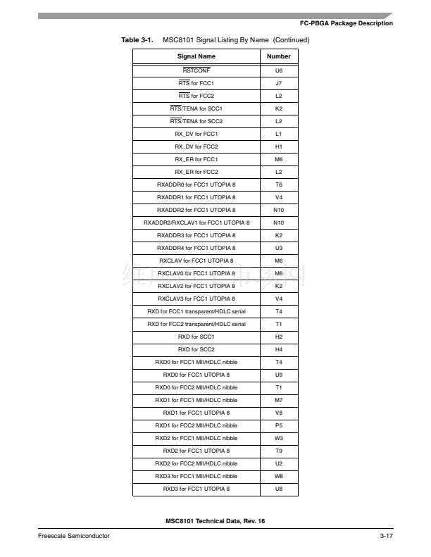
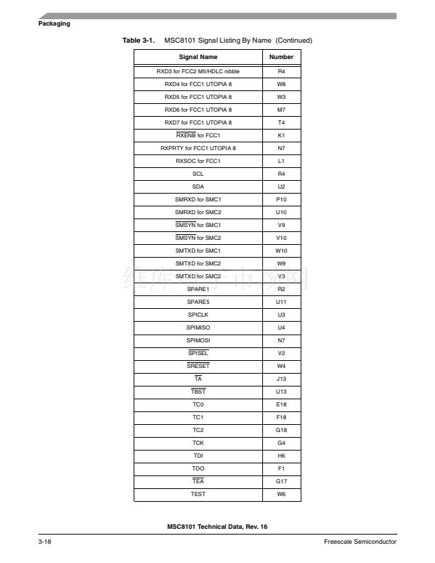
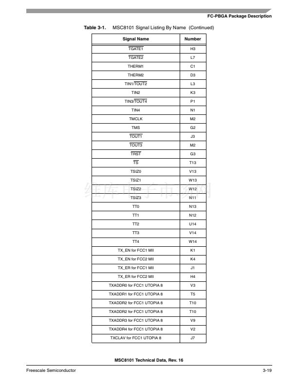
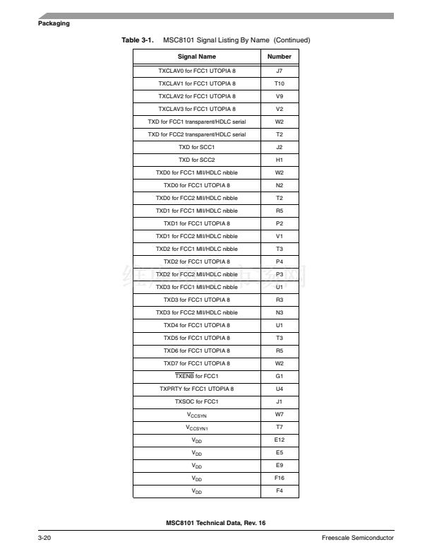
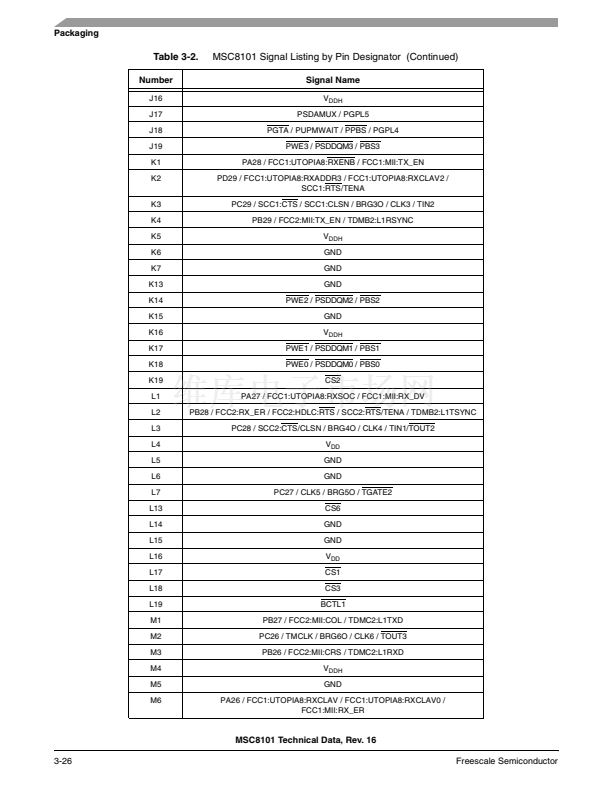
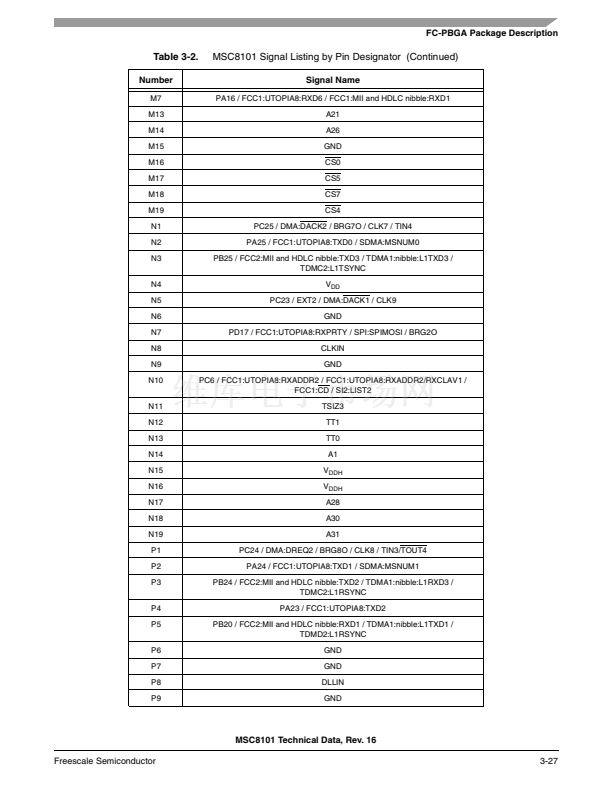
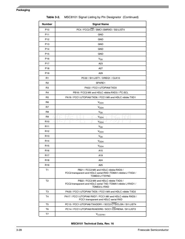
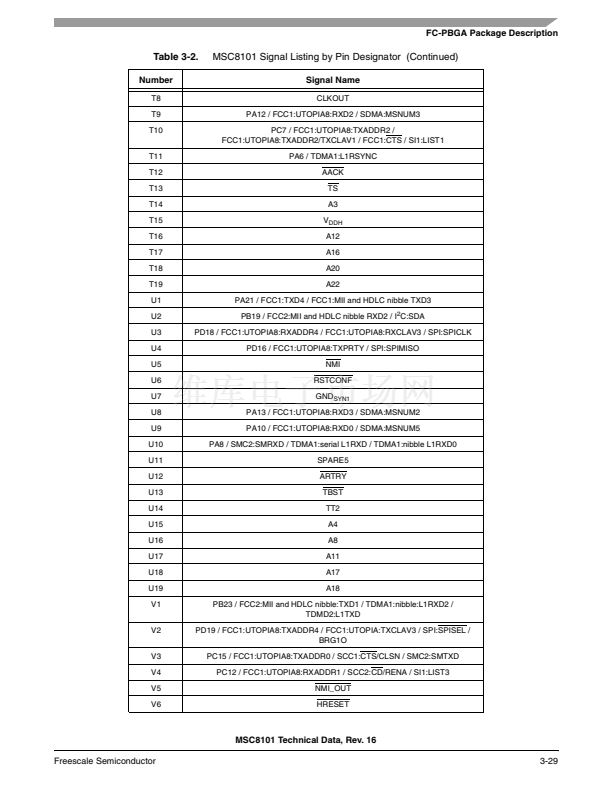
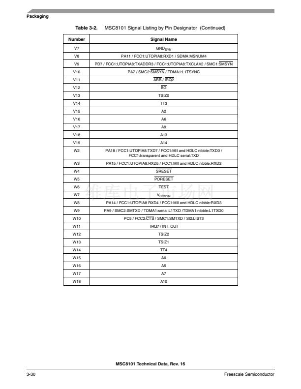
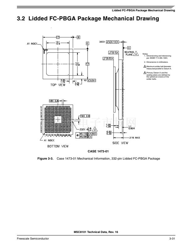
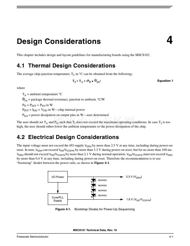
CPM Ports
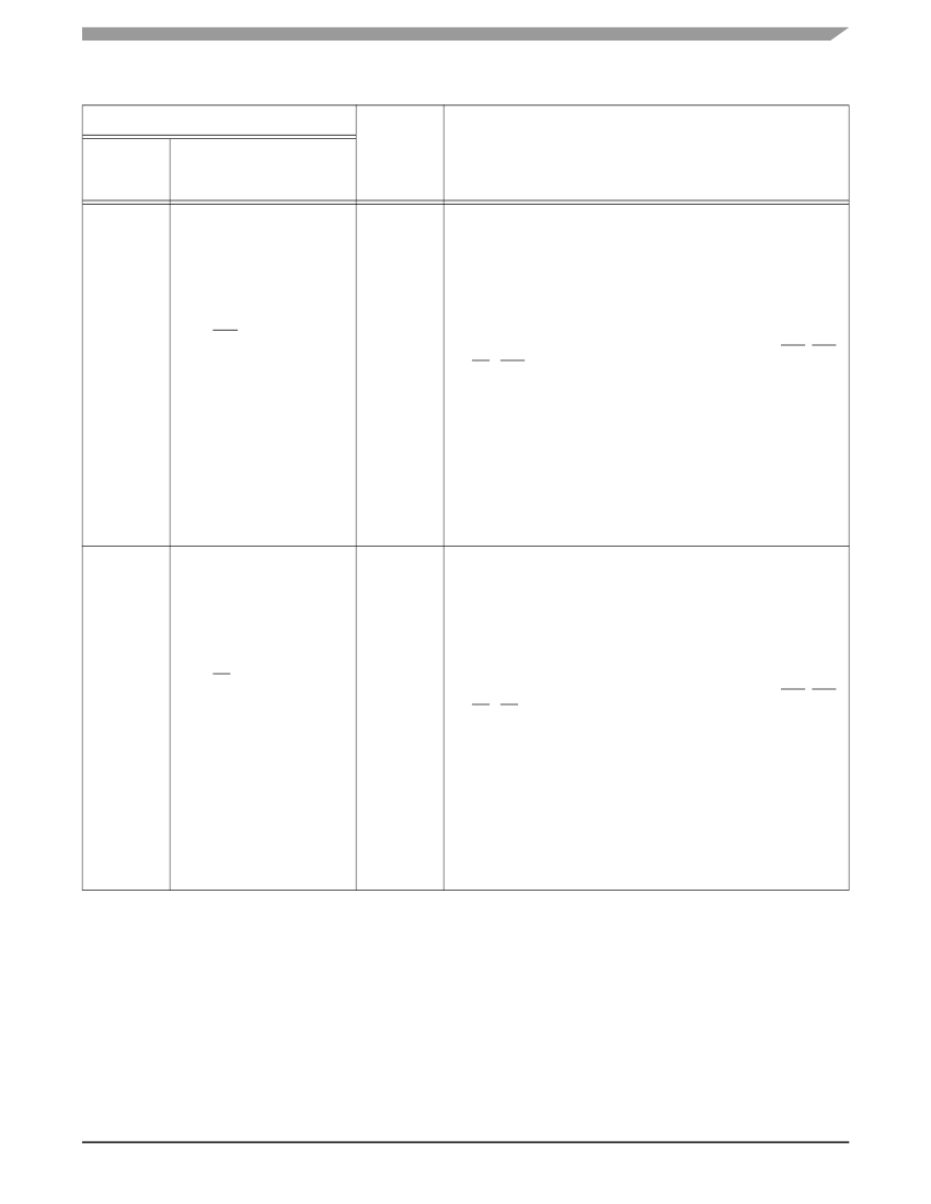
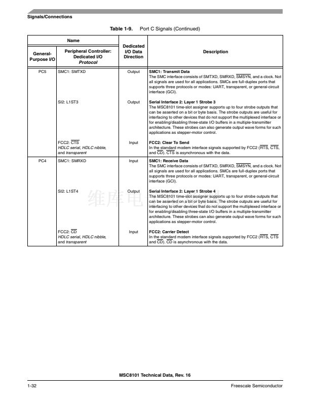
Table 1-9.
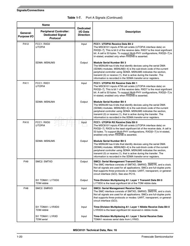
Name
General-
Purpose I/O
PC7
Port C Signals (Continued)
Peripheral Controller:
Dedicated I/O
Protocol
SI2: L1ST1
Dedicated
I/O Data
Direction
Output
Description
Serial Interface 2: Strobe 1
The MSC8101 time-slot assigner supports up to four strobe outputs that
can be asserted on a bit or byte basis. The strobe outputs are useful for
interfacing to other devices that do not support the multiplexed interface or
for enabling/disabling three-state I/O buffers in a multiple-transmitter
architecture. These strobes can also generate output wave forms for such
applications as stepper-motor control.
FCC1: Clear To Send
In the standard modem interface signals supported by FCC1 (RTS, CTS,
and CD). CTS is asynchronous with the data.
FCC1: UTOPIA Multi-PHY Master Transmit Address Bit 2
This is master transmit address bit 2.
FCC1: UTOPIA Multi-PHY Slave Transmit Address Bit 2
This is slave transmit address bit 2.
FCC1: UTOPIA Multi-PHY Master Transmit Cell Available 1 Direct
Polling
Asserted by an external UTOPIA slave PHY to indicate that it can accept
one complete ATM cell.
Serial Interface 2: Layer 1 Strobe 2
The MSC8101 time-slot assigner supports up to four strobe outputs that
can be asserted on a bit or byte basis. The strobe outputs are useful for
interfacing to other devices that do not support the multiplexed interface or
for enabling/disabling three-state I/O buffers in a multiple-transmitter
architecture. These strobes can also generate output wave forms for such
applications as stepper-motor control.
FCC1: Carrier Detect
In the standard modem interface signals supported by FCC1 (RTS, CTS,
and CD). CD is an input asynchronous with the data.
FCC1: UTOPIA Multi-PHY Master Receive Address Bit 2
This is master receive address bit 2.
FCC1: UTOPIA Slave Receive Address Bit 2
This is slave receive address bit 2.
FCC1: UTOPIA Multi-PHY Master Receive Cell Available 1 Direct
Polling
Asserted by an external PHY when one complete ATM cell is available for
transfer.
FCC1: CTS
HDLC serial, HDLC nibble,
and
transparent
FCC1: TXADDR2
UTOPIA master
FCC1: TXADDR2
UTOPIA slave
FCC1: TXCLAV1
UTOPIA multi-PHY master, direct
polling
PC6
SI2: L1ST2
Input
Output
Input
Input
Output
FCC1: CD
HDLC serial, HDLC nibble,
and
transparent
FCC1: RXADDR2
UTOPIA master
FCC1: RXADDR2
UTOPIA slave
FCC1: RXCLAV1
UTOPIA multi-PHY master, direct
polling
Input
Output
Input
Input
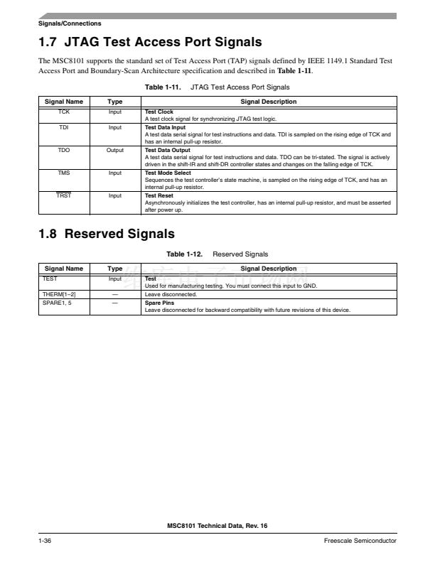
MSC8101 Technical Data, Rev. 16
Freescale Semiconductor
1-31


 1
1
 2
2
 3
3
 4
4
 5
5
 6
6
 7
7
 8
8
 9
9
 10
10
 11
11
 12
12
 13
13
 14
14
 15
15
 16
16
 17
17
 18
18
 19
19
 20
20
 21
21
 22
22
 23
23
 24
24
 25
25
 26
26
 27
27
 28
28
 29
29
 30
30
 31
31
 32
32
 33
33
 34
34
 35
35
 36
36
 37
37
 38
38
 39
39
 40
40
 41
41
 42
42
 43
43
 44
44
 45
45
 46
46
 47
47
 48
48
 49
49
 50
50
 51
51
 52
52
 53
53
 54
54
 55
55
 56
56
 57
57
 58
58
 59
59
 60
60
 61
61
 62
62
 63
63
 64
64
 65
65
 66
66
 67
67
 68
68
 69
69
 70
70
 71
71
 72
72
 73
73
 74
74
 75
75
 76
76
 77
77
 78
78
 79
79
 80
80
 81
81
 82
82
 83
83
 84
84
 85
85
 86
86
 87
87
 88
88
 89
89
 90
90
 91
91
 92
92
 93
93
 94
94
 95
95
 96
96
 97
97
 98
98
 99
99
 100
100
 101
101
 102
102
 103
103
 104
104
