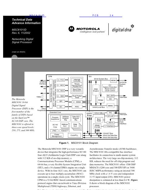
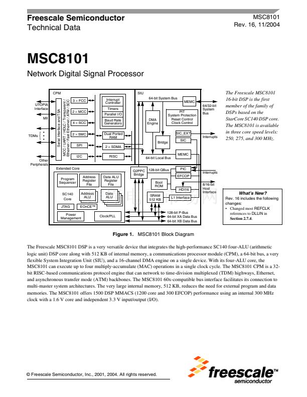
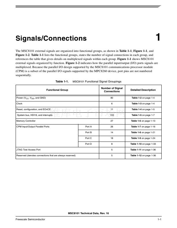
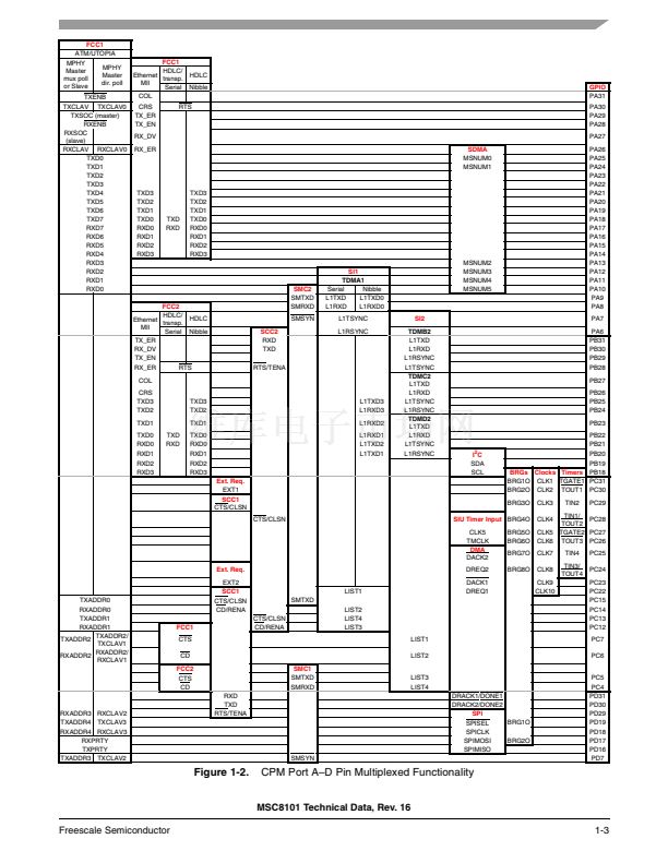
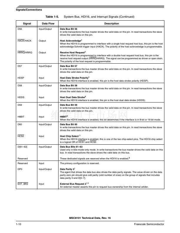
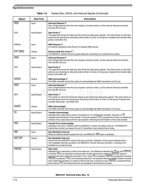
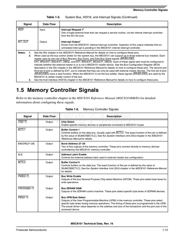
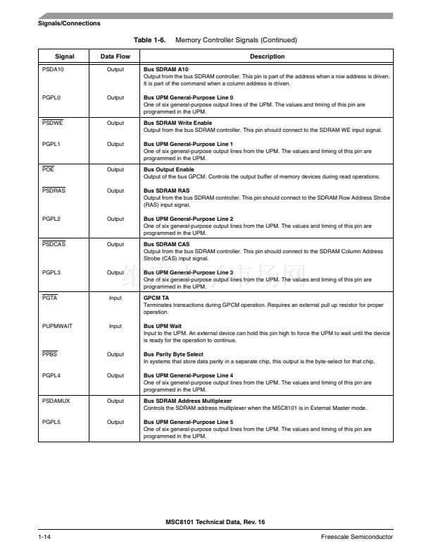
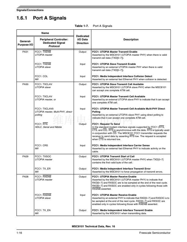
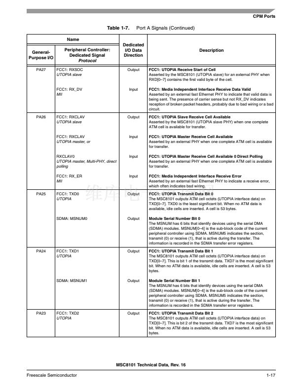
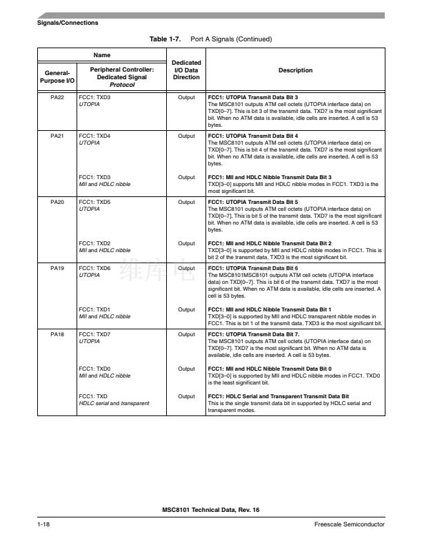
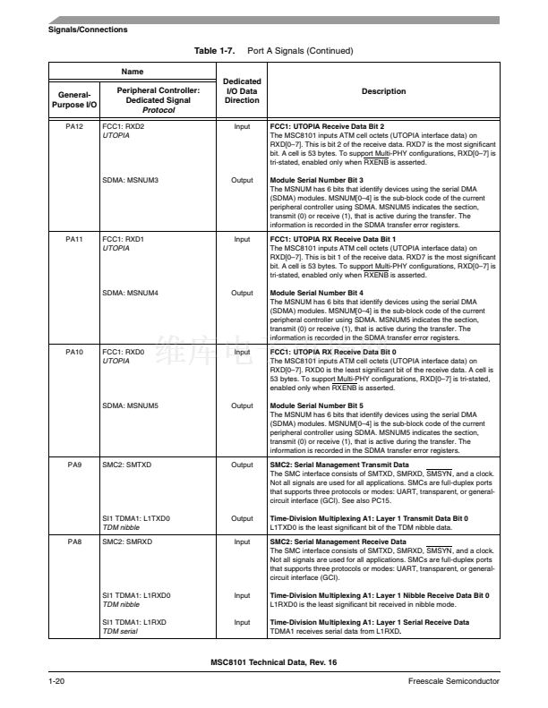
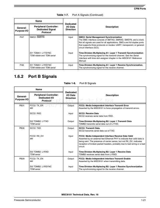
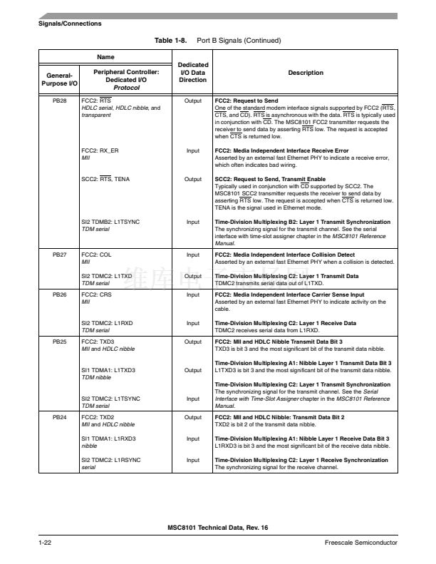
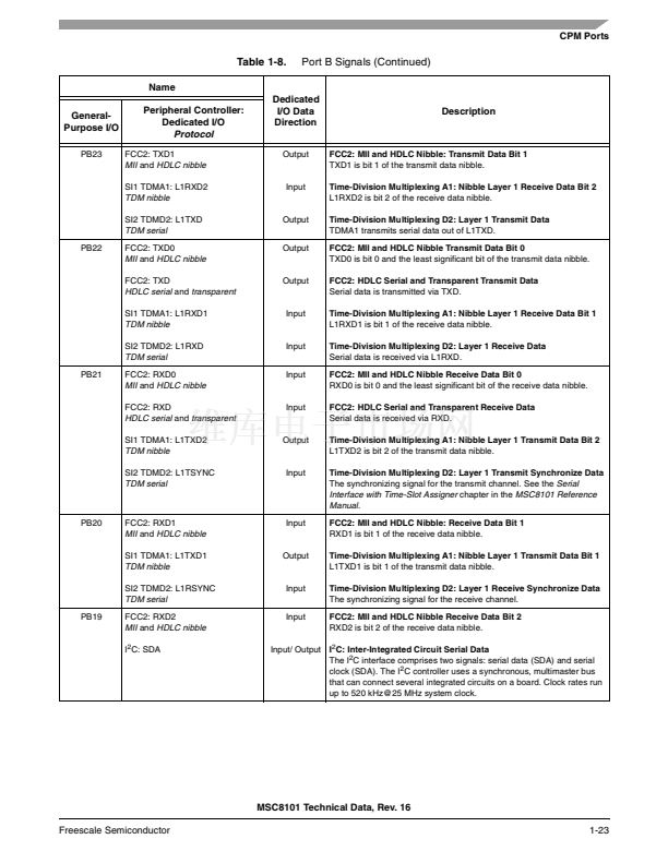
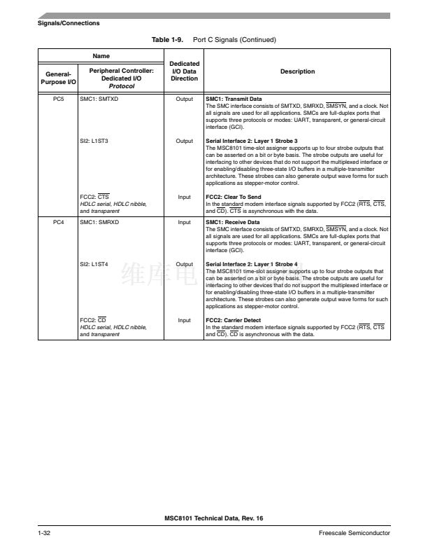
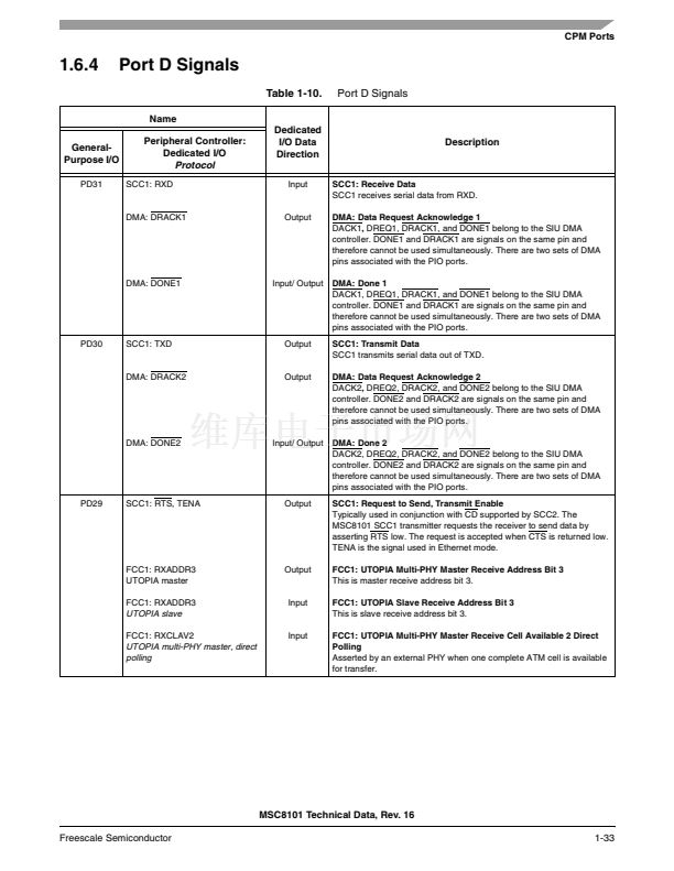
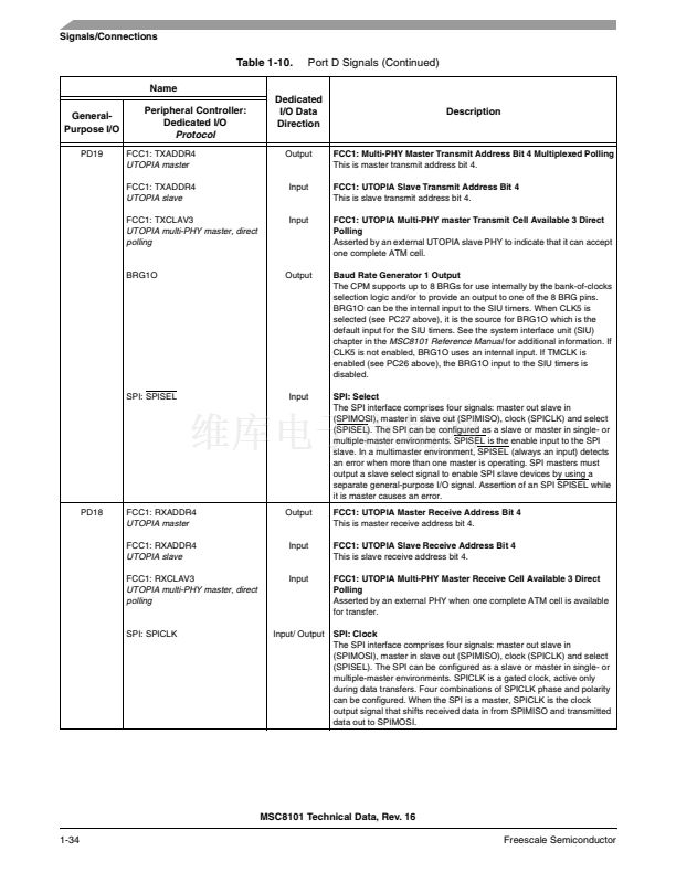
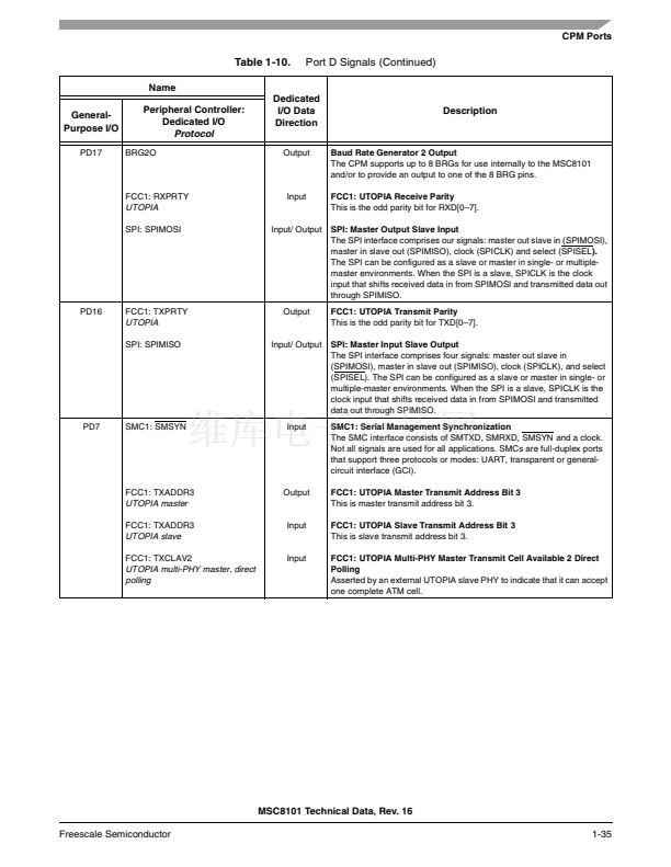
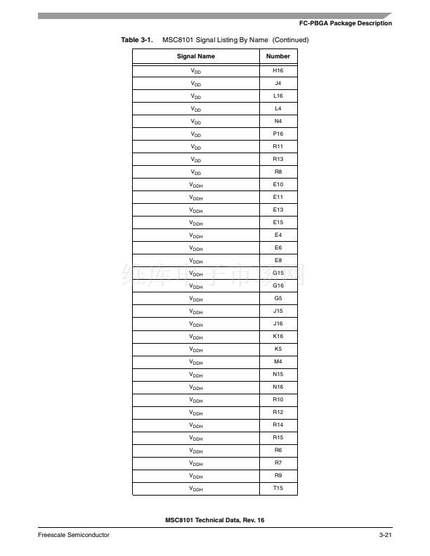
Signals/Connections
1.1 Power Signals
Table 1-2.
Power Name
V
DD
Power and Ground Signal Inputs
Description
Internal Logic Power
V
DD
dedicated for use with the device core. The voltage should be well-regulated and the input should be provided with
an extremely low impedance path to the V
DD
power rail.
Input/Output Power
This source supplies power for the I/O buffers. The user must provide adequate external decoupling capacitors.
System PLL Power
V
CC
dedicated for use with the system Phase Lock Loop (PLL). The voltage should be well-regulated and the input
should be provided with an extremely low impedance path to the V
CC
power rail.
SC140 PLL Power
V
CC
dedicated for use with the SC140 core PLL. The voltage should be well-regulated and the input should be provided
with an extremely low impedance path to the V
CC
power rail.
System Ground
An isolated ground for the internal processing logic. This connection must be tied externally to all chip ground
connections, except GND
SYN
and GND
SYN1
. The user must provide adequate external decoupling capacitors.
System PLL Ground
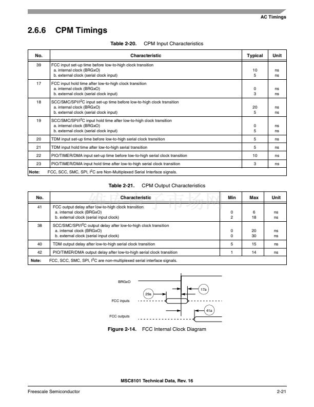
Ground dedicated for system PLL use. The connection should be provided with an extremely low-impedance path to
ground.
SC140 PLL Ground 1
Ground dedicated for SC140 core PLL use. The connection should be provided with an extremely low-impedance path
to ground.
V
DDH
V
CCSYN
V
CCSYN1
GND
GND
SYN
GND
SYN1
1.2 Clock Signals
Table 1-3.
Signal Name
CLKIN
MODCK1
Input
Input
Clock Signals
Signal Description
Type
Clock In
Primary clock input to the MSC8101 PLL.
Clock Mode Input 1
Defines the operating mode of internal clock circuits.
Transfer Code 0
Supplies information that can be useful for debugging bus transactions initiated by the MSC8101.
Bank Select 0
Selects the SDRAM bank when the MSC8101 is in 60x-compatible bus mode.
Clock Mode Input 2
Defines the operating mode of internal clock circuits.
Transfer Code 1
Supplies information that can be useful for debugging bus transactions initiated by the MSC8101.
Bank Select 1
Selects the SDRAM bank when the MSC8101 is in 60x-compatible bus mode.
Clock Mode Input 3
Defines the operating mode of internal clock circuits.
Transfer Code 2
Supplies information that can be useful for debugging bus transactions initiated by the MSC8101.
Bank Select 2
Selects the SDRAM bank when the MSC8101 is in 60x-compatible bus mode.
TC0
Output
BNKSEL0
MODCK2
Output
Input
TC1
Output
BNKSEL1
MODCK3
Output
Input
TC2
Output
BNKSEL2
Output
MSC8101 Technical Data, Rev. 16
1-4
Freescale Semiconductor


 1
1
 2
2
 3
3
 4
4
 5
5
 6
6
 7
7
 8
8
 9
9
 10
10
 11
11
 12
12
 13
13
 14
14
 15
15
 16
16
 17
17
 18
18
 19
19
 20
20
 21
21
 22
22
 23
23
 24
24
 25
25
 26
26
 27
27
 28
28
 29
29
 30
30
 31
31
 32
32
 33
33
 34
34
 35
35
 36
36
 37
37
 38
38
 39
39
 40
40
 41
41
 42
42
 43
43
 44
44
 45
45
 46
46
 47
47
 48
48
 49
49
 50
50
 51
51
 52
52
 53
53
 54
54
 55
55
 56
56
 57
57
 58
58
 59
59
 60
60
 61
61
 62
62
 63
63
 64
64
 65
65
 66
66
 67
67
 68
68
 69
69
 70
70
 71
71
 72
72
 73
73
 74
74
 75
75
 76
76
 77
77
 78
78
 79
79
 80
80
 81
81
 82
82
 83
83
 84
84
 85
85
 86
86
 87
87
 88
88
 89
89
 90
90
 91
91
 92
92
 93
93
 94
94
 95
95
 96
96
 97
97
 98
98
 99
99
 100
100
 101
101
 102
102
 103
103
 104
104
