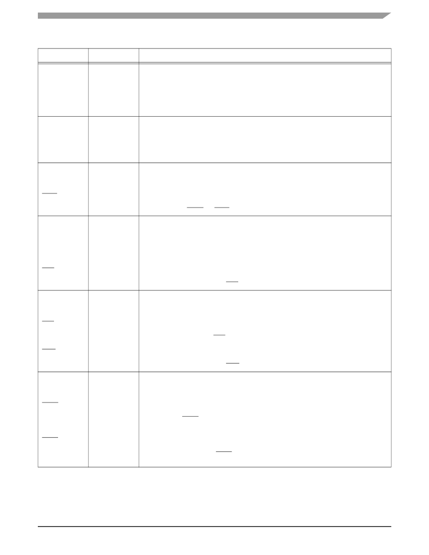
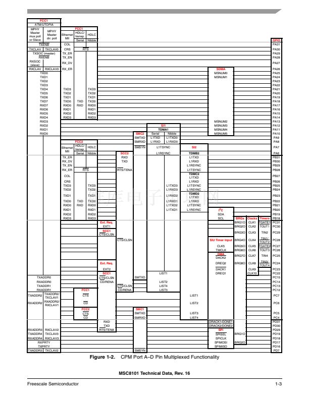
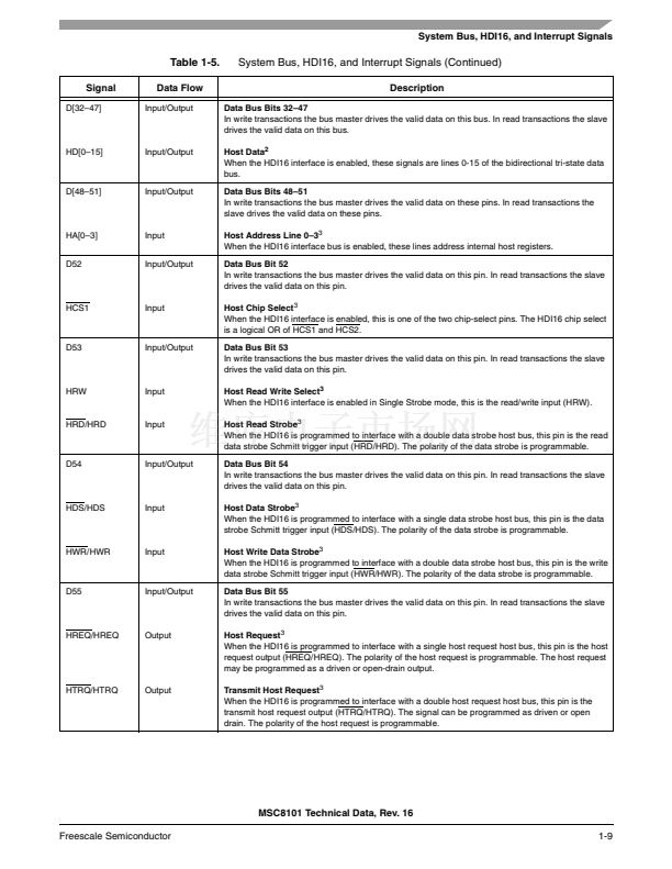
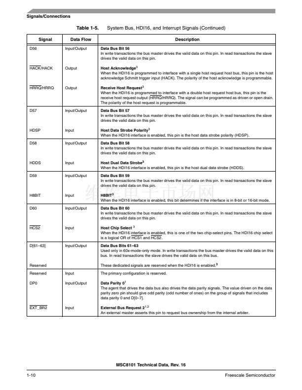
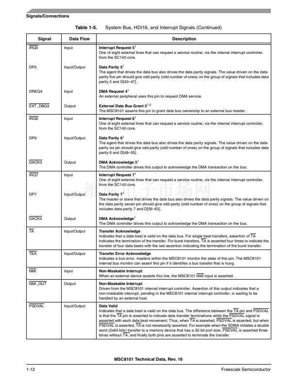
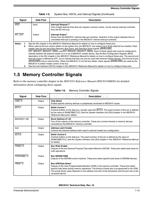
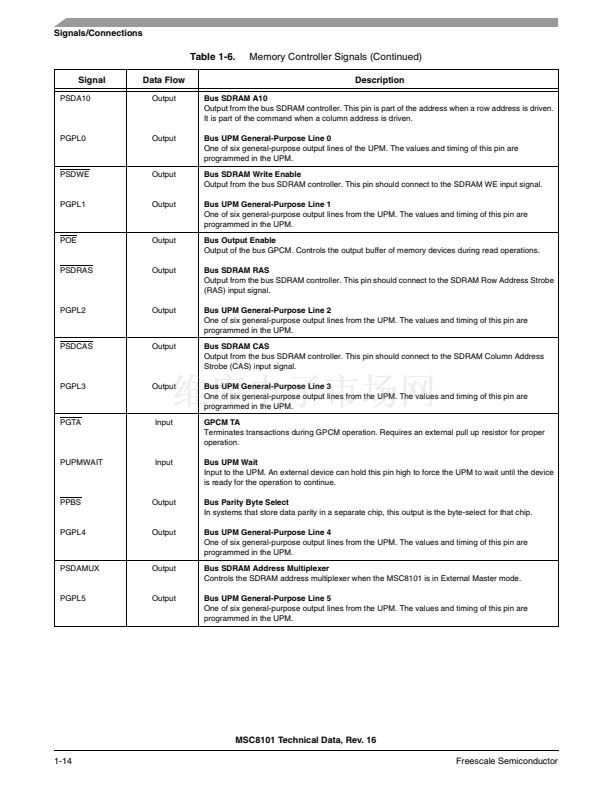
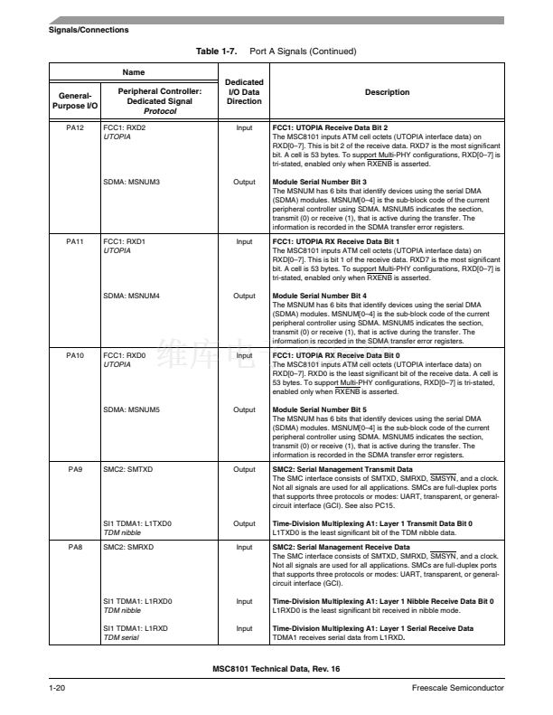
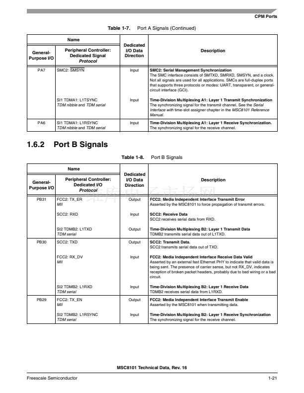
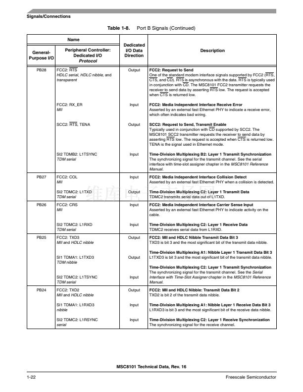
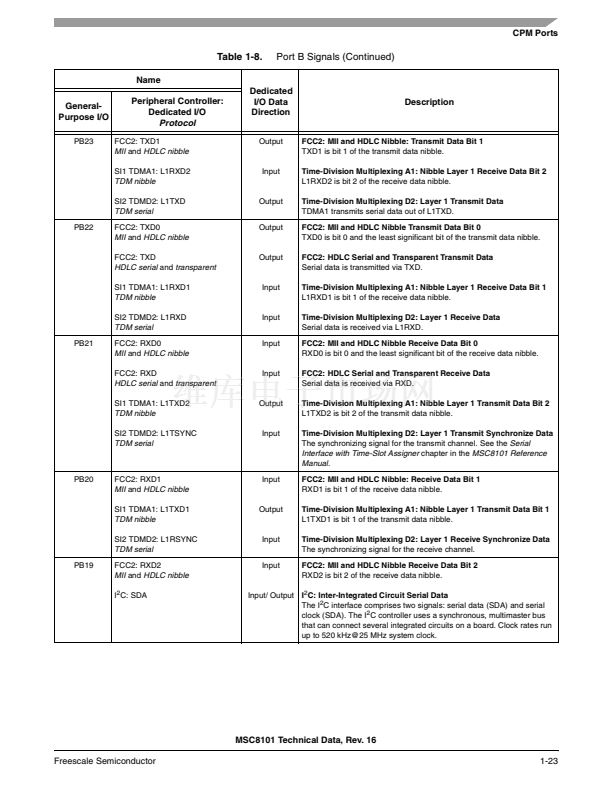
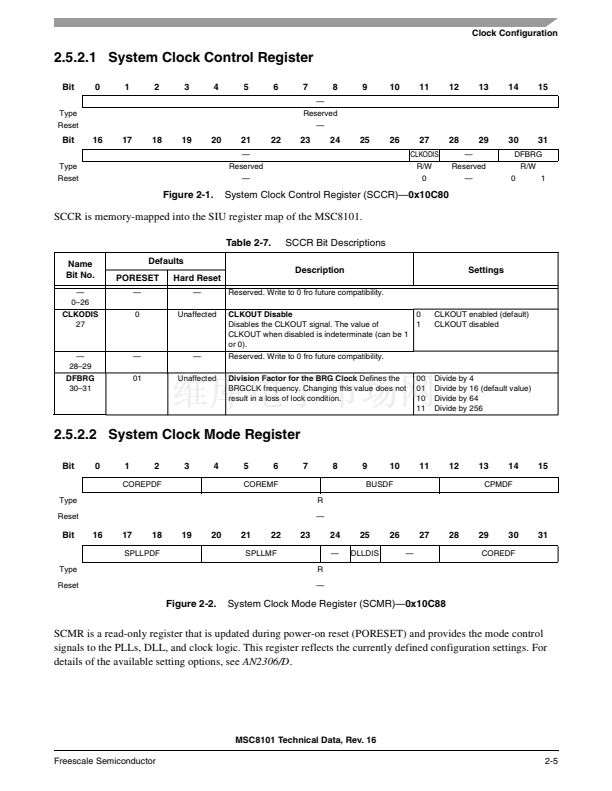
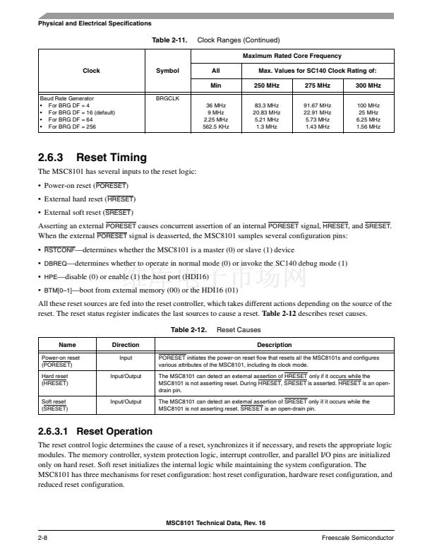
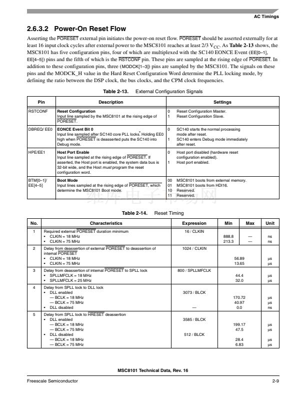
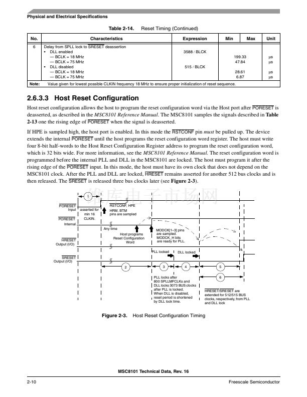
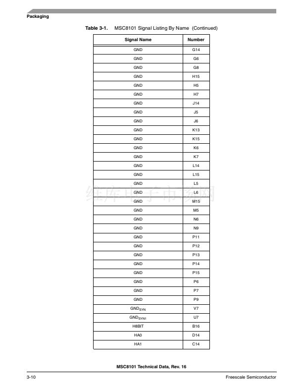
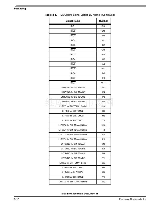
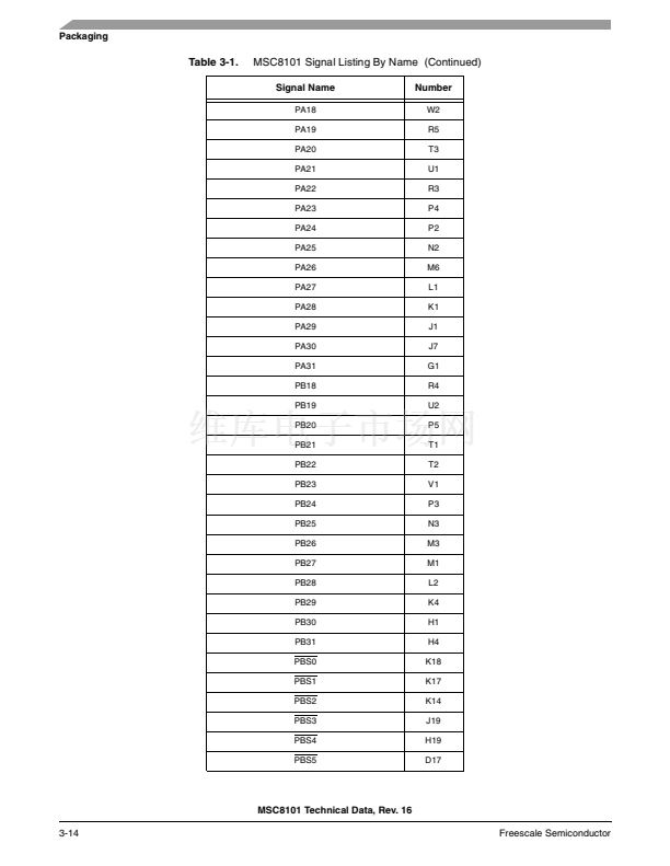
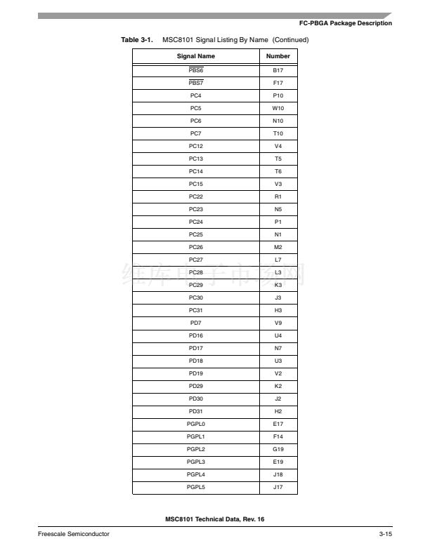
System Bus, HDI16, and Interrupt Signals
Table 1-5.
Signal
D[32鈥?7]
System Bus, HDI16, and Interrupt Signals (Continued)
Description
Data Bus Bits 32鈥?7
In write transactions the bus master drives the valid data on this bus. In read transactions the slave
drives the valid data on this bus.
Host Data
2
When the HDI16 interface is enabled, these signals are lines 0-15 of the bidirectional tri-state data
bus.
Data Bus Bits 48鈥?1
In write transactions the bus master drives the valid data on these pins. In read transactions the
slave drives the valid data on these pins.
Host Address Line 0鈥?
3
When the HDI16 interface bus is enabled, these lines address internal host registers.
Data Bus Bit 52
In write transactions the bus master drives the valid data on this pin. In read transactions the slave
drives the valid data on this pin.
Host Chip Select
3
When the HDI16 interface is enabled, this is one of the two chip-select pins. The HDI16 chip select
is a logical OR of HCS1 and HCS2.
Data Bus Bit 53
In write transactions the bus master drives the valid data on this pin. In read transactions the slave
drives the valid data on this pin.
Host Read Write Select
3
When the HDI16 interface is enabled in Single Strobe mode, this is the read/write input (HRW).
Host Read Strobe
3
When the HDI16 is programmed to interface with a double data strobe host bus, this pin is the read
data strobe Schmitt trigger input (HRD/HRD). The polarity of the data strobe is programmable.
Data Bus Bit 54
In write transactions the bus master drives the valid data on this pin. In read transactions the slave
drives the valid data on this pin.
Host Data Strobe
3
When the HDI16 is programmed to interface with a single data strobe host bus, this pin is the data
strobe Schmitt trigger input (HDS/HDS). The polarity of the data strobe is programmable.
Host Write Data Strobe
3
When the HDI16 is programmed to interface with a double data strobe host bus, this pin is the write
data strobe Schmitt trigger input (HWR/HWR). The polarity of the data strobe is programmable.
Data Bus Bit 55
In write transactions the bus master drives the valid data on this pin. In read transactions the slave
drives the valid data on this pin.
Host Request
3
When the HDI16 is programmed to interface with a single host request host bus, this pin is the host
request output (HREQ/HREQ). The polarity of the host request is programmable. The host request
may be programmed as a driven or open-drain output.
Transmit Host Request
3
When the HDI16 is programmed to interface with a double host request host bus, this pin is the
transmit host request output (HTRQ/HTRQ). The signal can be programmed as driven or open
drain. The polarity of the host request is programmable.
Data Flow
Input/Output
HD[0鈥?5]
Input/Output
D[48鈥?1]
Input/Output
HA[0鈥?]
D52
Input
Input/Output
HCS1
Input
D53
Input/Output
HRW
Input
HRD/HRD
Input
D54
Input/Output
HDS/HDS
Input
HWR/HWR
Input
D55
Input/Output
HREQ/HREQ
Output
HTRQ/HTRQ
Output
MSC8101 Technical Data, Rev. 16
Freescale Semiconductor
1-9


 1
1
 2
2
 3
3
 4
4
 5
5
 6
6
 7
7
 8
8
 9
9
 10
10
 11
11
 12
12
 13
13
 14
14
 15
15
 16
16
 17
17
 18
18
 19
19
 20
20
 21
21
 22
22
 23
23
 24
24
 25
25
 26
26
 27
27
 28
28
 29
29
 30
30
 31
31
 32
32
 33
33
 34
34
 35
35
 36
36
 37
37
 38
38
 39
39
 40
40
 41
41
 42
42
 43
43
 44
44
 45
45
 46
46
 47
47
 48
48
 49
49
 50
50
 51
51
 52
52
 53
53
 54
54
 55
55
 56
56
 57
57
 58
58
 59
59
 60
60
 61
61
 62
62
 63
63
 64
64
 65
65
 66
66
 67
67
 68
68
 69
69
 70
70
 71
71
 72
72
 73
73
 74
74
 75
75
 76
76
 77
77
 78
78
 79
79
 80
80
 81
81
 82
82
 83
83
 84
84
 85
85
 86
86
 87
87
 88
88
 89
89
 90
90
 91
91
 92
92
 93
93
 94
94
 95
95
 96
96
 97
97
 98
98
 99
99
 100
100
 101
101
 102
102
 103
103
 104
104
