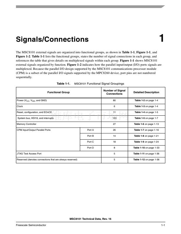
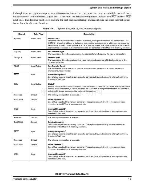
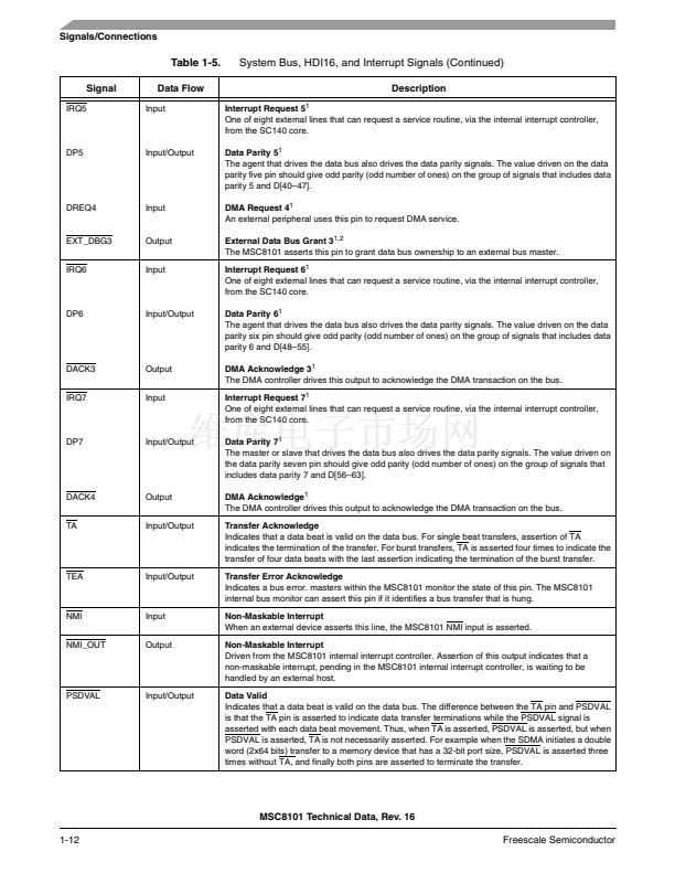
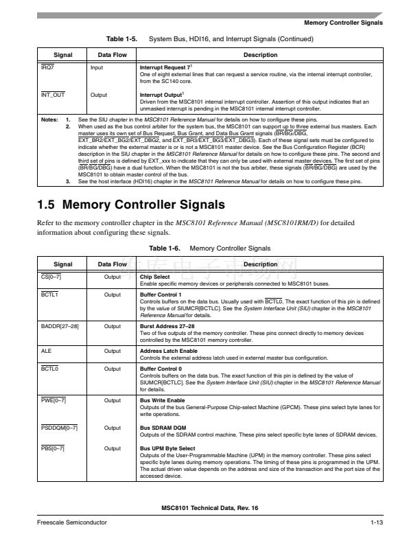
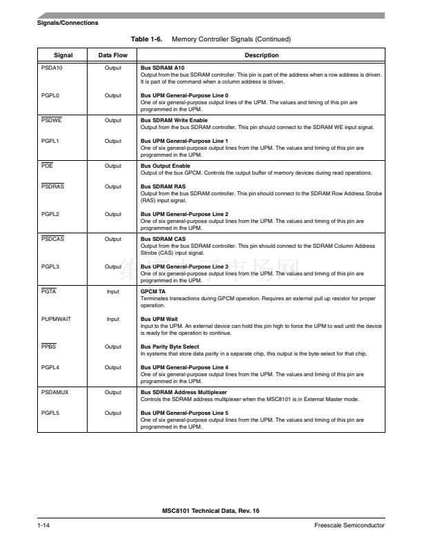
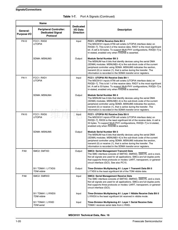
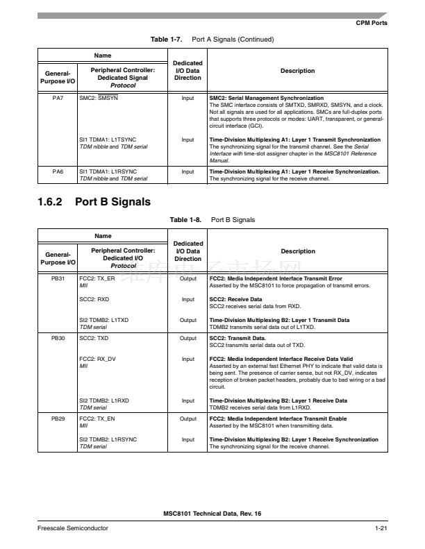
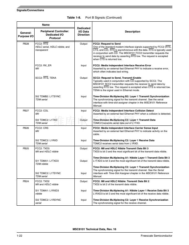
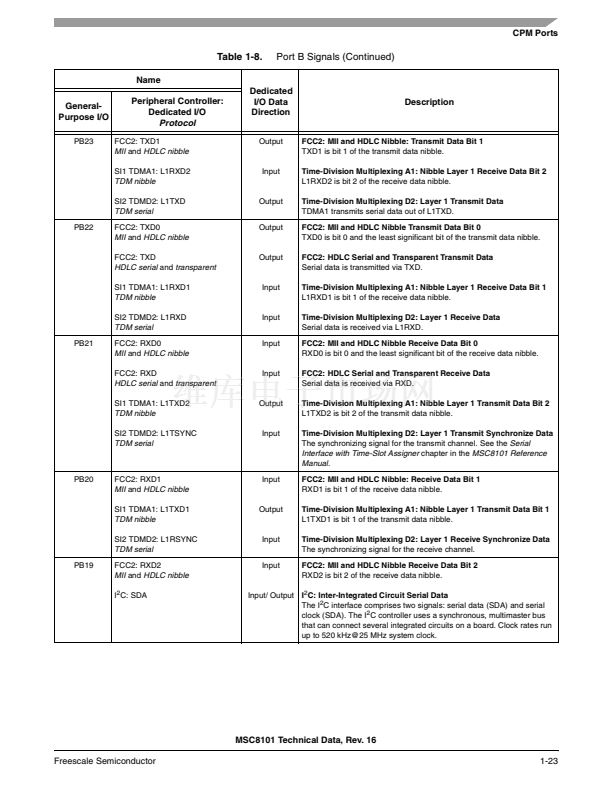
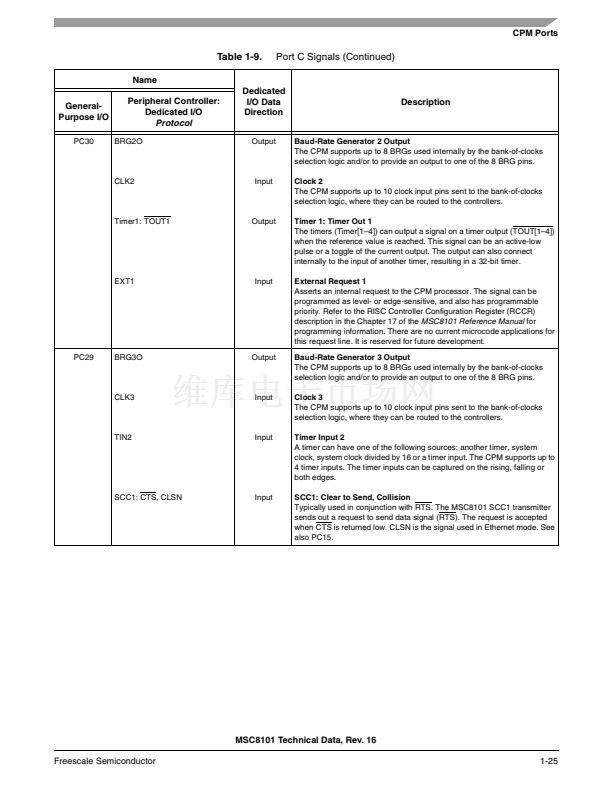
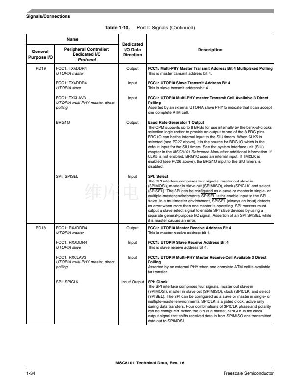
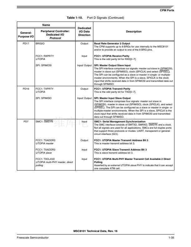
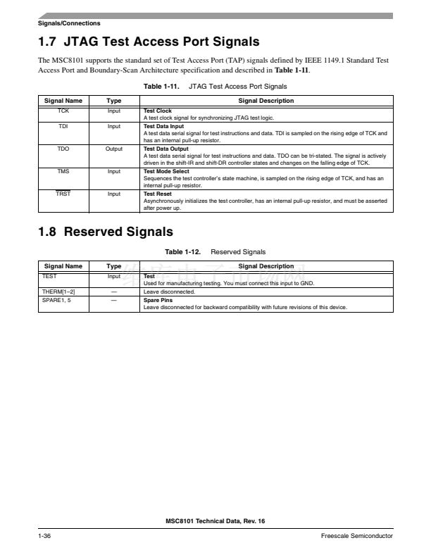
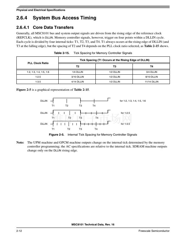
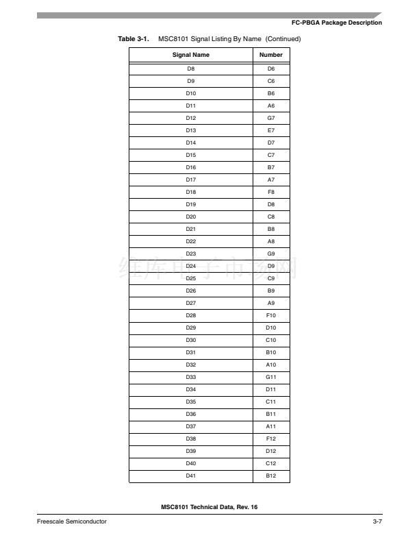
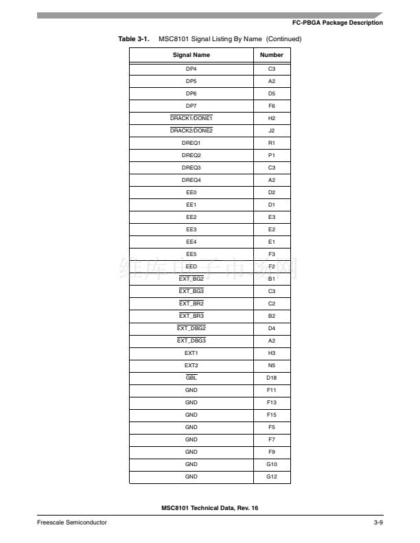
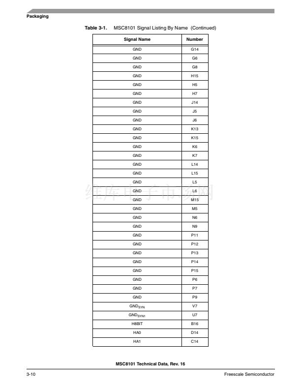
CPM Ports
Table 1-9.
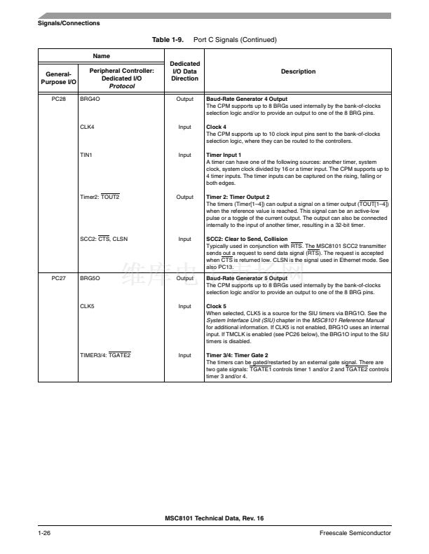
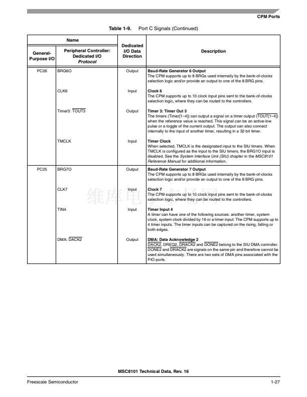
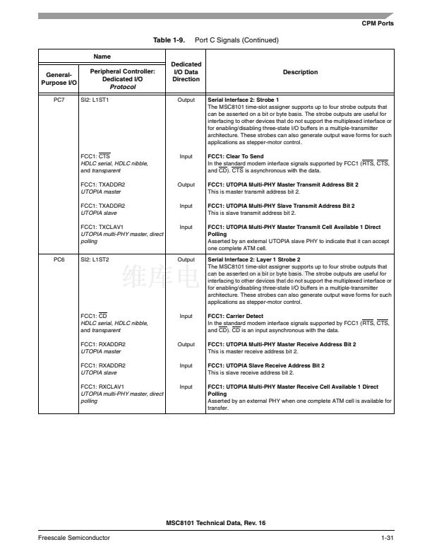
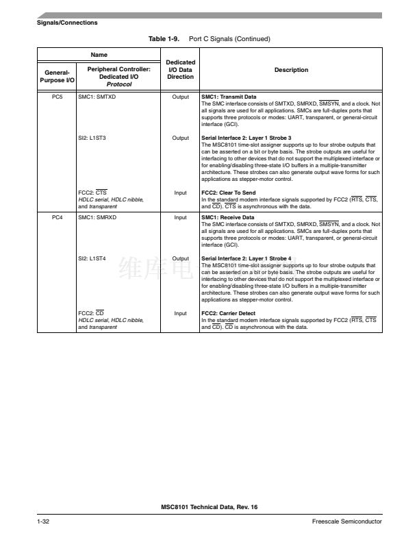
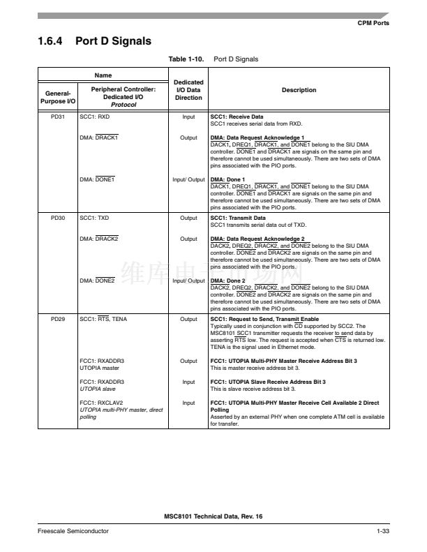
Name
General-
Purpose I/O
PC26
Port C Signals (Continued)
Peripheral Controller:
Dedicated I/O
Protocol
BRG6O
Dedicated
I/O Data
Direction
Output
Description
Baud-Rate Generator 6 Output
The CPM supports up to 8 BRGs used internally by the bank-of-clocks
selection logic and/or provide an output to one of the 8 BRG pins.
Clock 6
The CPM supports up to 10 clock input pins sent to the bank-of-clocks
selection logic, where they can be routed to the controllers.
Timer 3: Timer Out 3
The timers (Timer[1鈥?]) can output a signal on a timer output (TOUT[1鈥?])
when the reference value is reached. This signal can be an active-low
pulse or a toggle of the current output. The output can also connect
internally to the input of another timer, resulting in a 32-bit timer.
Timer Clock
When selected, TMCLK is the designated input to the SIU timers. When
TMCLK is configured as the input to the SIU timers, the BRG1O input is
disabled. See the
System Interface Unit (SIU)
chapter in the
MSC8101
Reference Manual
for additional information.
Baud-Rate Generator 7 Output
The CPM supports up to 8 BRGs used internally by the bank-of-clocks
selection logic and/or provide an output to one of the 8 BRG pins.
Clock 7
The CPM supports up to 10 clock input pins sent to the bank-of-clocks
selection logic, where they can be routed to the controllers.
Timer Input 4
A timer can have one of the following sources: another timer, system
clock, system clock divided by 16 or a timer input. The CPM supports up to
4 timer inputs. The timer inputs can be captured on the rising, falling or
both edges.
DMA: Data Acknowledge 2
DACK2, DREQ2, DRACK2 and DONE2 belong to the SIU DMA controller.
DONE2 and DRACK2 are signals on the same pin and therefore cannot be
used simultaneously. There are two sets of DMA pins associated with the
PIO ports.
CLK6
Input
Timer3: TOUT3
Output
TMCLK
Input
PC25
BRG7O
Output
CLK7
Input
TIN4
Input
DMA: DACK2
Output
MSC8101 Technical Data, Rev. 16
Freescale Semiconductor
1-27


 1
1
 2
2
 3
3
 4
4
 5
5
 6
6
 7
7
 8
8
 9
9
 10
10
 11
11
 12
12
 13
13
 14
14
 15
15
 16
16
 17
17
 18
18
 19
19
 20
20
 21
21
 22
22
 23
23
 24
24
 25
25
 26
26
 27
27
 28
28
 29
29
 30
30
 31
31
 32
32
 33
33
 34
34
 35
35
 36
36
 37
37
 38
38
 39
39
 40
40
 41
41
 42
42
 43
43
 44
44
 45
45
 46
46
 47
47
 48
48
 49
49
 50
50
 51
51
 52
52
 53
53
 54
54
 55
55
 56
56
 57
57
 58
58
 59
59
 60
60
 61
61
 62
62
 63
63
 64
64
 65
65
 66
66
 67
67
 68
68
 69
69
 70
70
 71
71
 72
72
 73
73
 74
74
 75
75
 76
76
 77
77
 78
78
 79
79
 80
80
 81
81
 82
82
 83
83
 84
84
 85
85
 86
86
 87
87
 88
88
 89
89
 90
90
 91
91
 92
92
 93
93
 94
94
 95
95
 96
96
 97
97
 98
98
 99
99
 100
100
 101
101
 102
102
 103
103
 104
104
