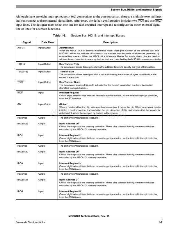
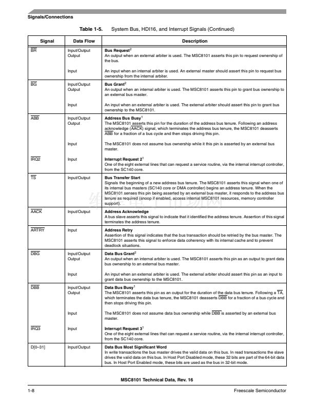
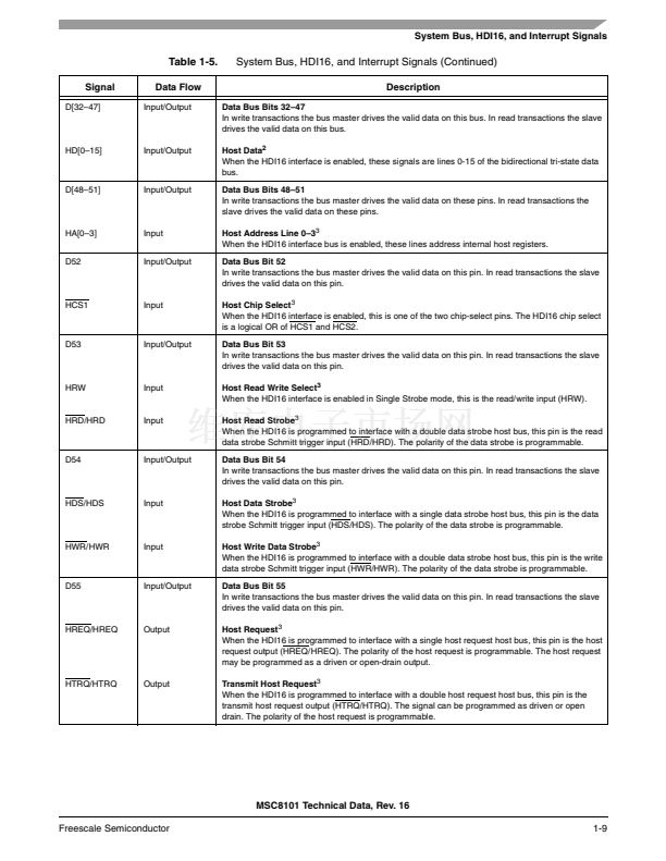
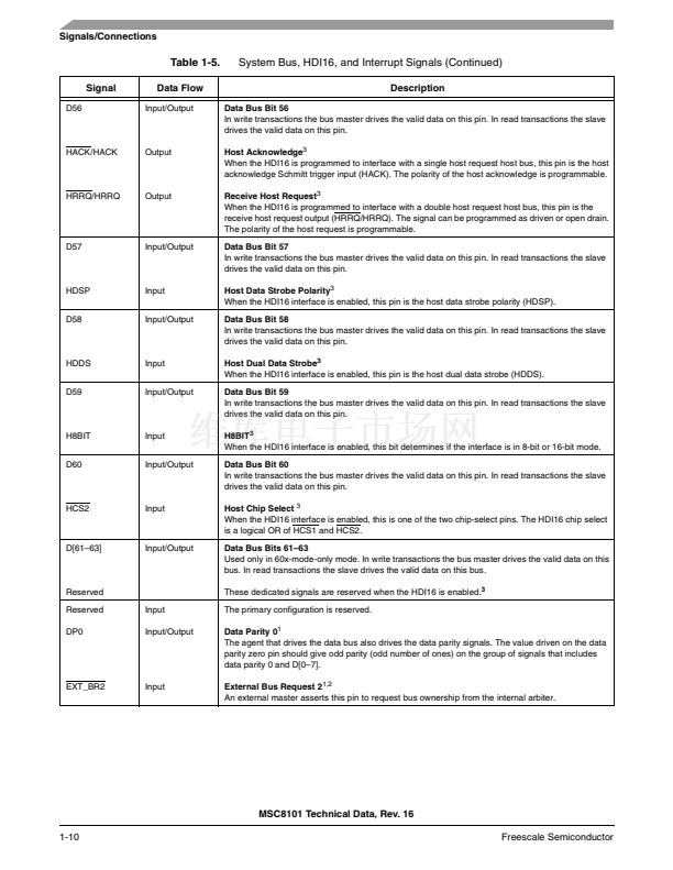
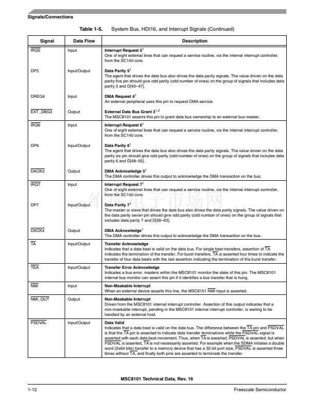
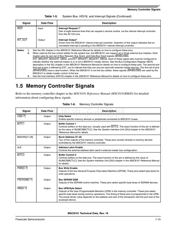
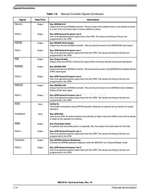
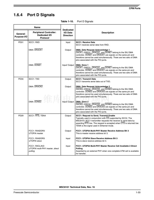
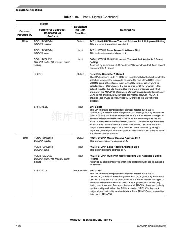
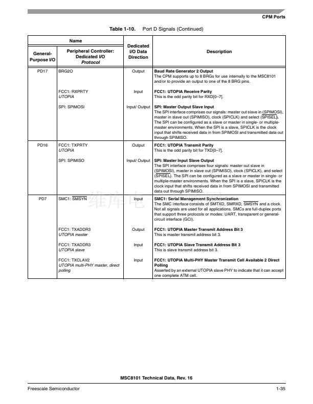
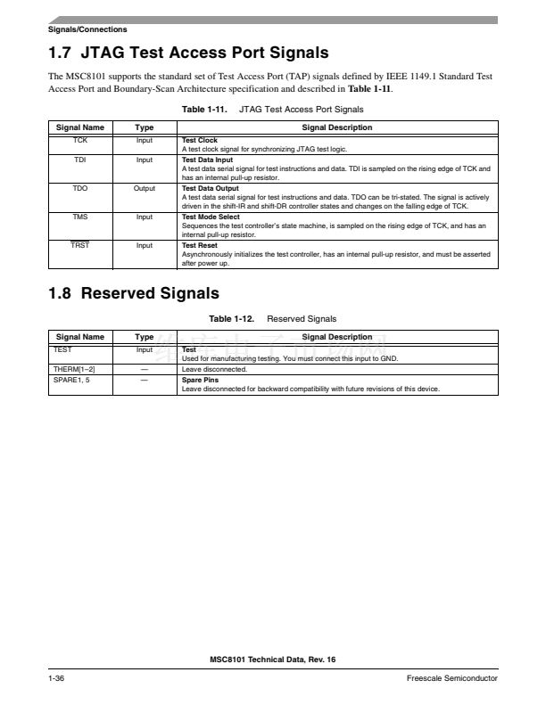
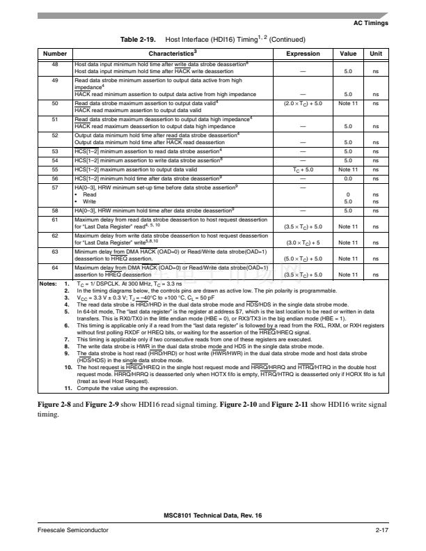
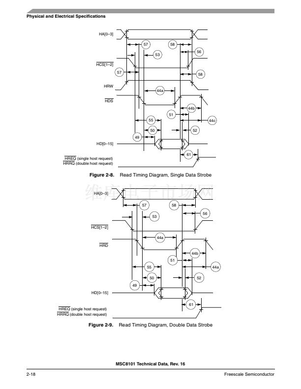
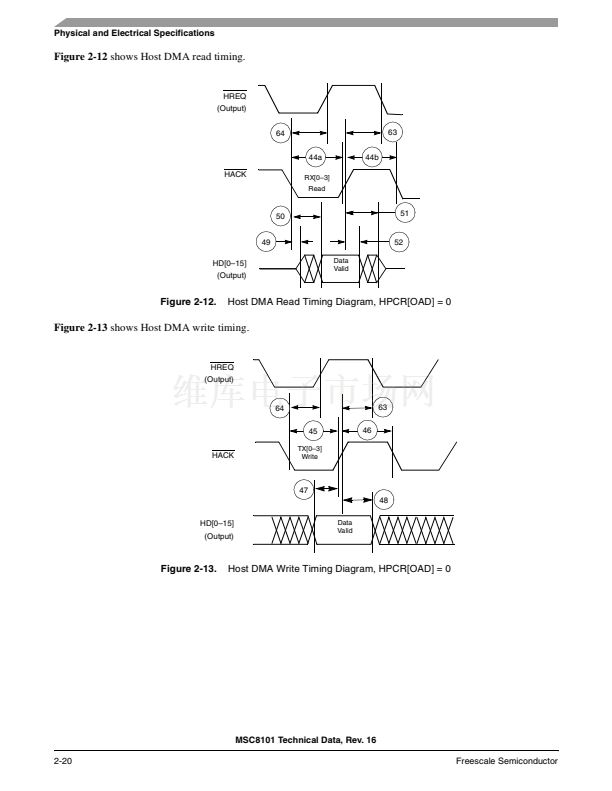
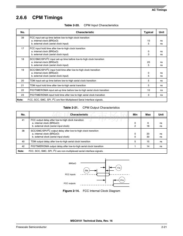
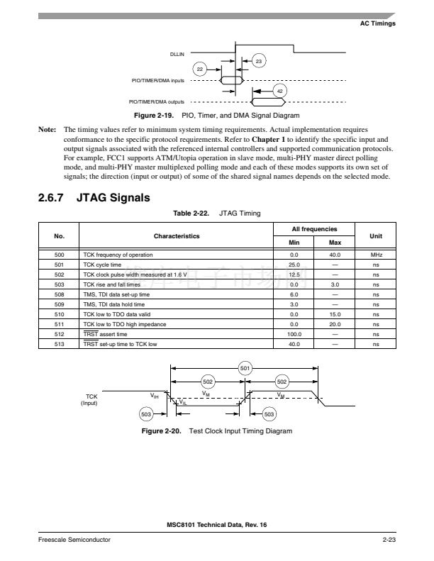
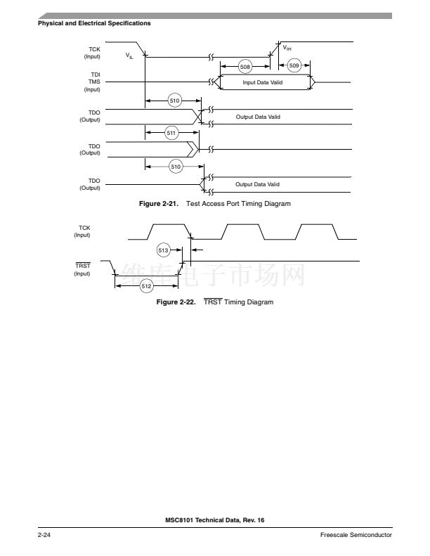
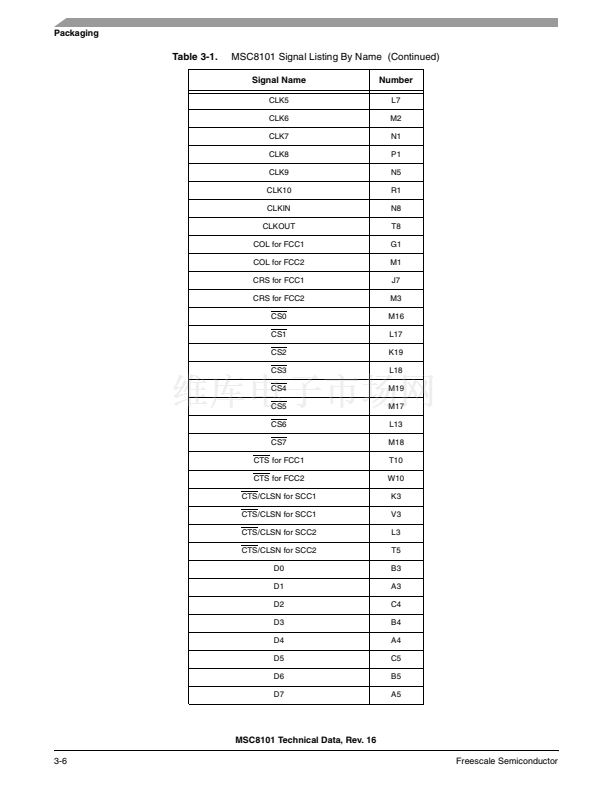
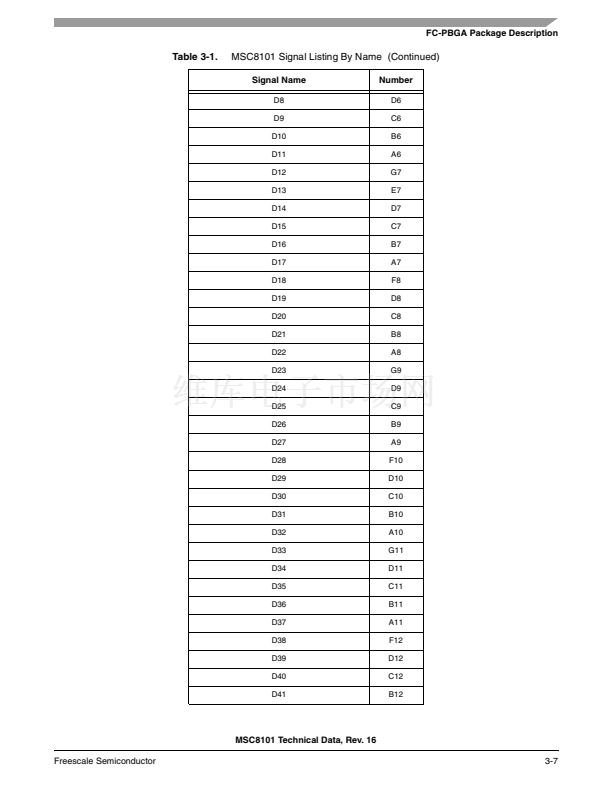
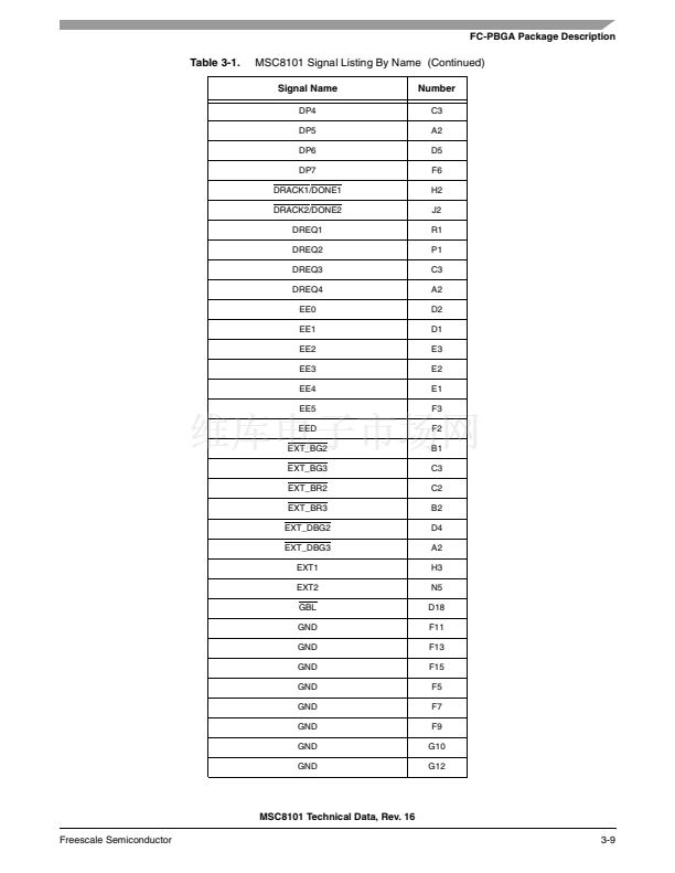
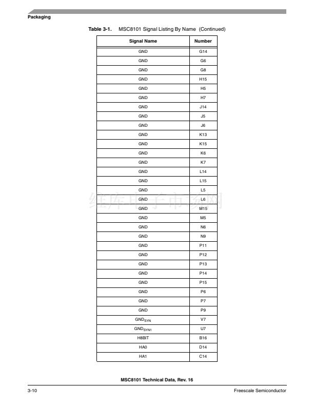
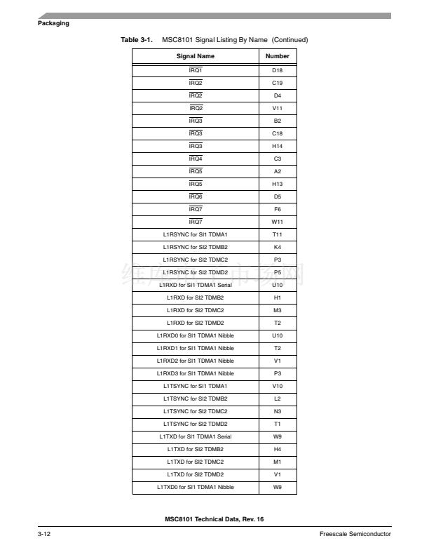
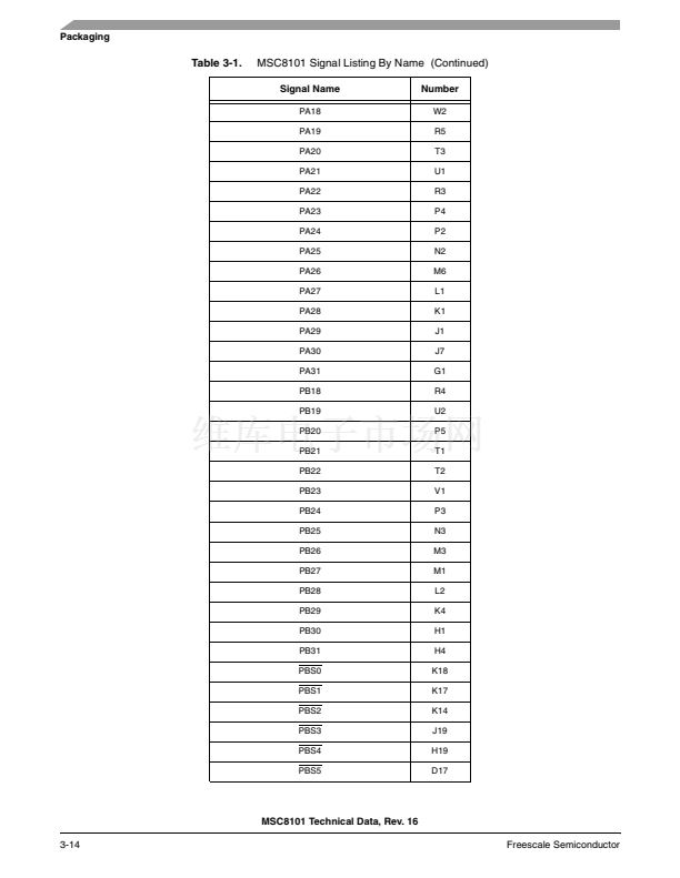
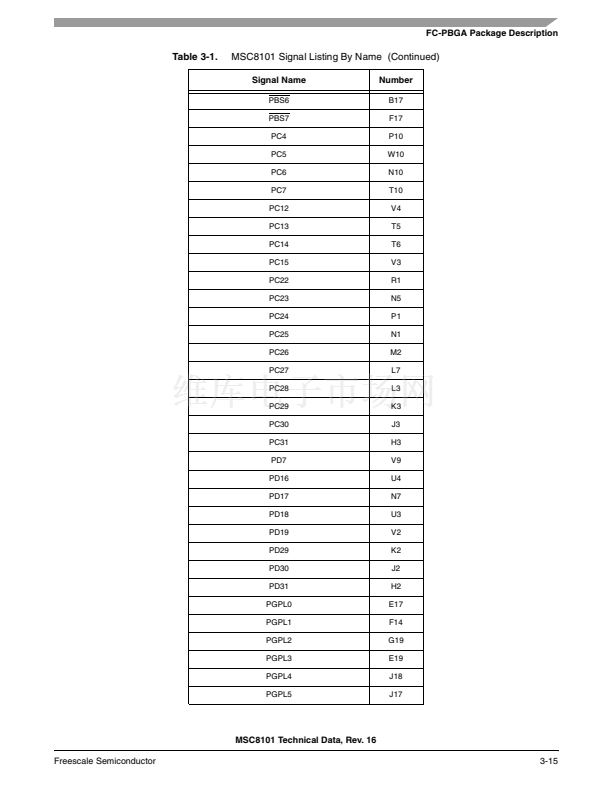
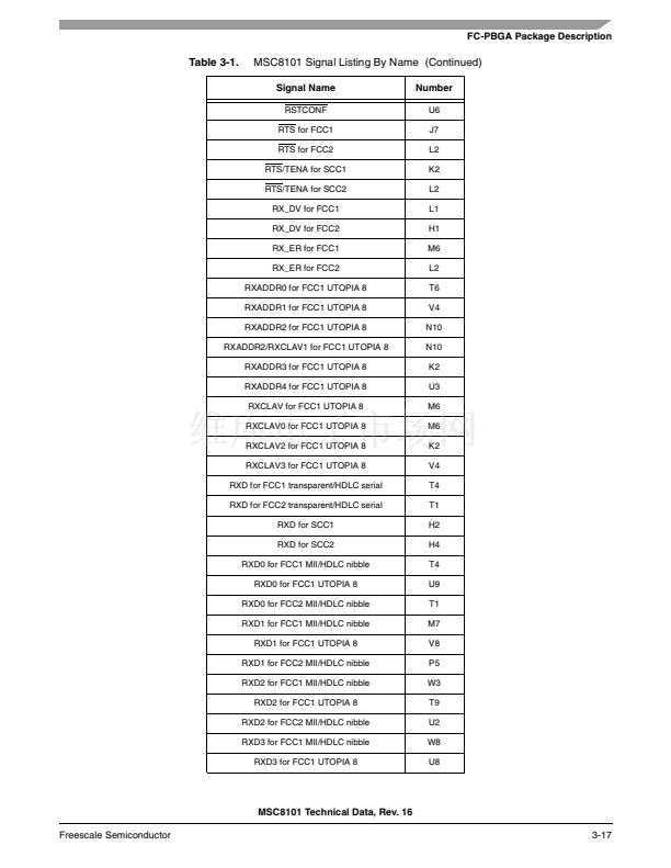
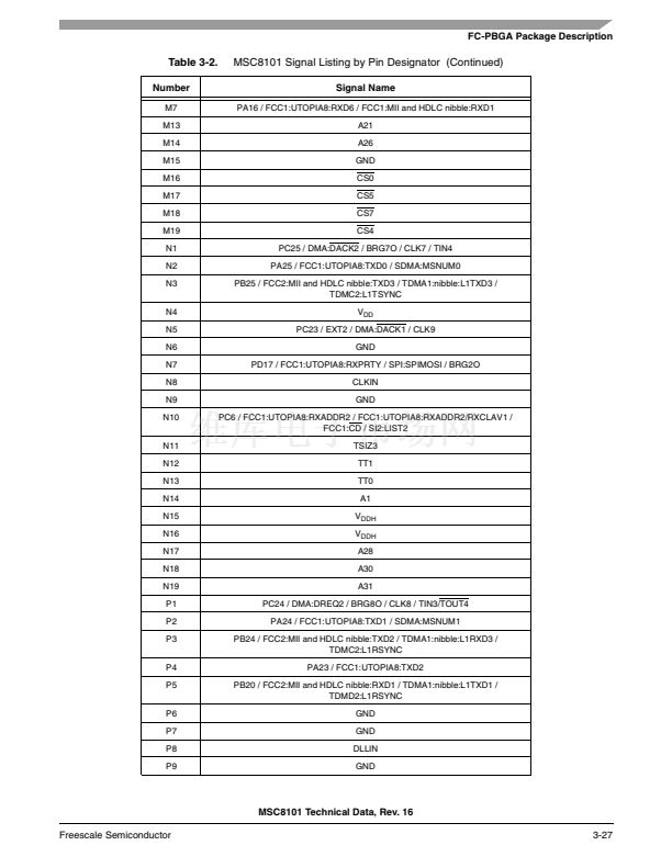
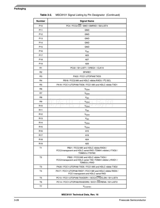
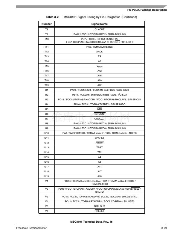
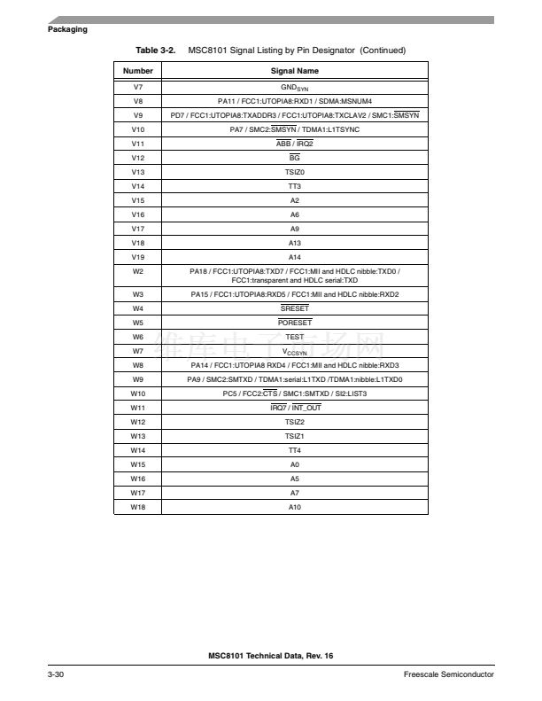
Signals/Connections
1
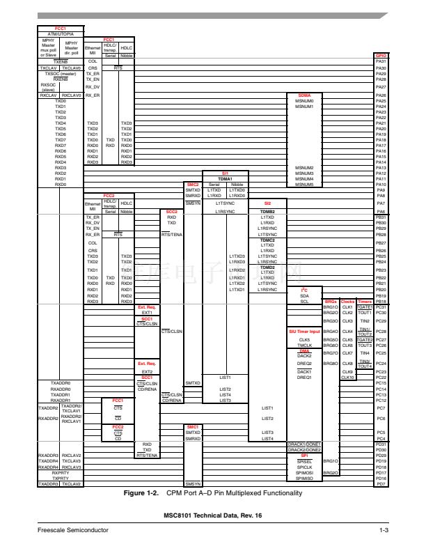
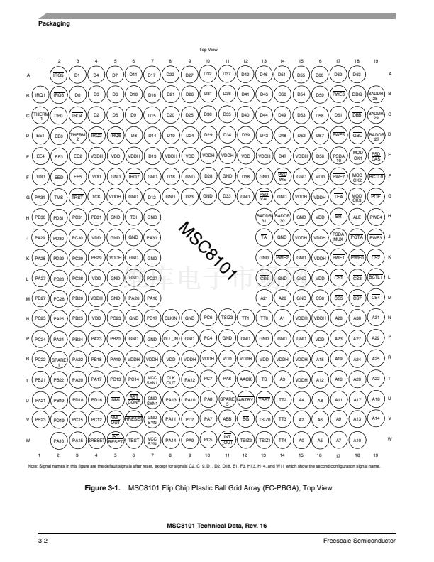
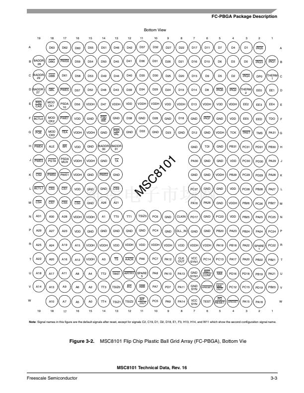
The MSC8101 external signals are organized into functional groups, as shown in
Table 1-1, Figure 1-1,
and
Figure 1-2. Table 1-1
lists the functional groups, states the number of signal connections in each group, and
references the table that gives details on multiplexed signals within each group.
Figure 1-1
shows MSC8101
external signals organized by function.
Figure 1-2
indicates how the parallel input/output (I/O) ports signals are
multiplexed. Because the parallel I/O design supported by the MSC8101 communications processor module
(CPM) is a subset of the parallel I/O signals supported by the MPC8260 device, port pins are not numbered
sequentially.
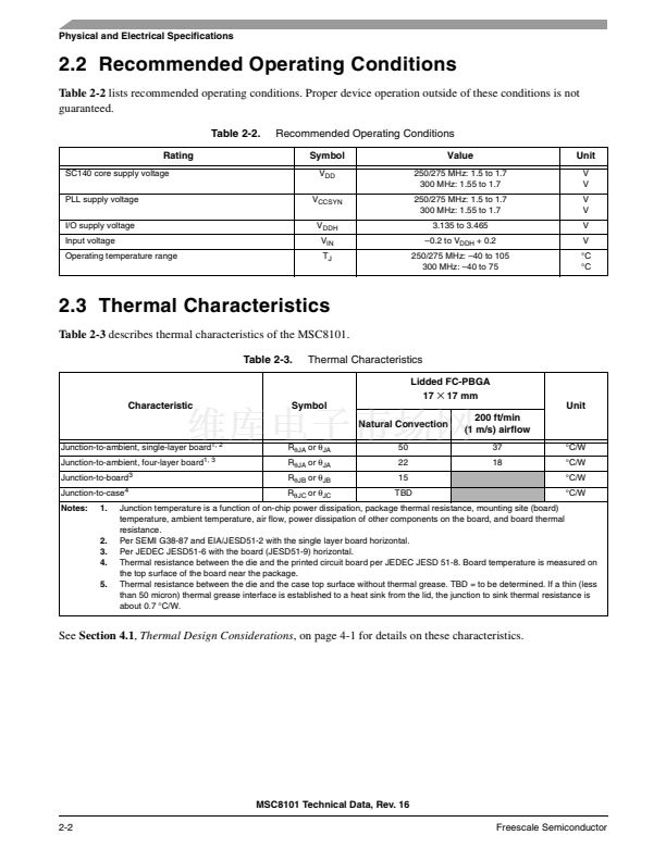
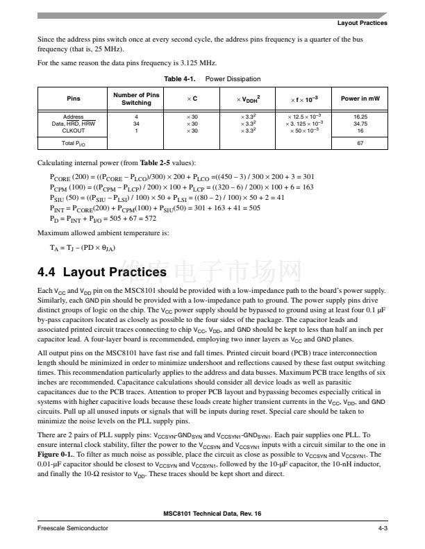
Table 1-1.
Functional Group
Power (V
CC
, V
DD
, and GND)
Clock
Reset, configuration, and EOnCE
System bus, HDI16, and interrupts
Memory Controller
CPM Input/Output Parallel Ports
Port A
Port B
Port C
Port D
JTAG Test Access Port
Reserved (denotes connections that are always reserved)
MSC8101
Functional Signal Groupings
Number of Signal
Connections
80
6
11
133
27
26
14
18
8
5
5
Detailed Description
Table 1-2
on page 1-4
Table 1-3
on page 1-4
Table 1-4
on page 1-5
Table 1-5
on page 1-7
Table 1-6
on page 1-13
Table 1-7
on page 1-16
Table 1-8
on page 1-21
Table 1-9
on page 1-24
Table 1-10
on page 1-33
Table 1-11
on page 1-36
Table 1-12
on page 1-36
MSC8101 Technical Data, Rev. 16
Freescale Semiconductor
1-1


 1
1
 2
2
 3
3
 4
4
 5
5
 6
6
 7
7
 8
8
 9
9
 10
10
 11
11
 12
12
 13
13
 14
14
 15
15
 16
16
 17
17
 18
18
 19
19
 20
20
 21
21
 22
22
 23
23
 24
24
 25
25
 26
26
 27
27
 28
28
 29
29
 30
30
 31
31
 32
32
 33
33
 34
34
 35
35
 36
36
 37
37
 38
38
 39
39
 40
40
 41
41
 42
42
 43
43
 44
44
 45
45
 46
46
 47
47
 48
48
 49
49
 50
50
 51
51
 52
52
 53
53
 54
54
 55
55
 56
56
 57
57
 58
58
 59
59
 60
60
 61
61
 62
62
 63
63
 64
64
 65
65
 66
66
 67
67
 68
68
 69
69
 70
70
 71
71
 72
72
 73
73
 74
74
 75
75
 76
76
 77
77
 78
78
 79
79
 80
80
 81
81
 82
82
 83
83
 84
84
 85
85
 86
86
 87
87
 88
88
 89
89
 90
90
 91
91
 92
92
 93
93
 94
94
 95
95
 96
96
 97
97
 98
98
 99
99
 100
100
 101
101
 102
102
 103
103
 104
104
