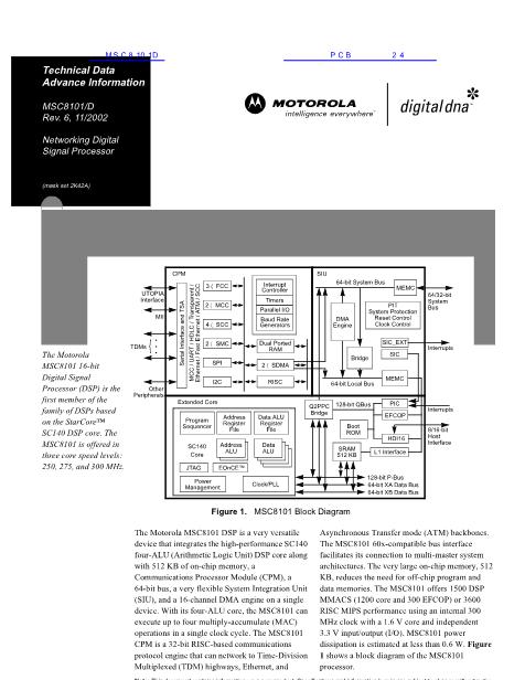
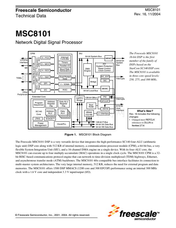
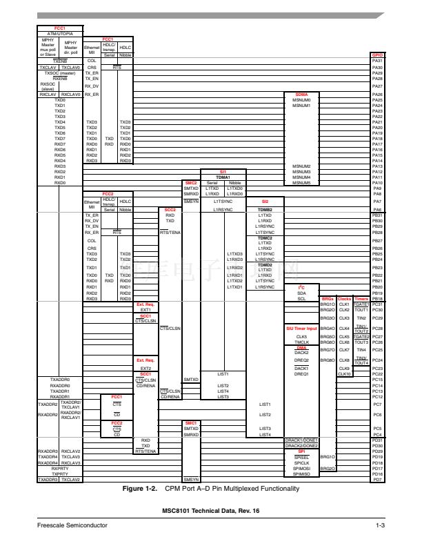
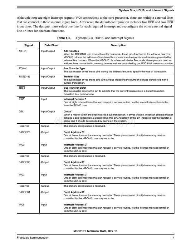
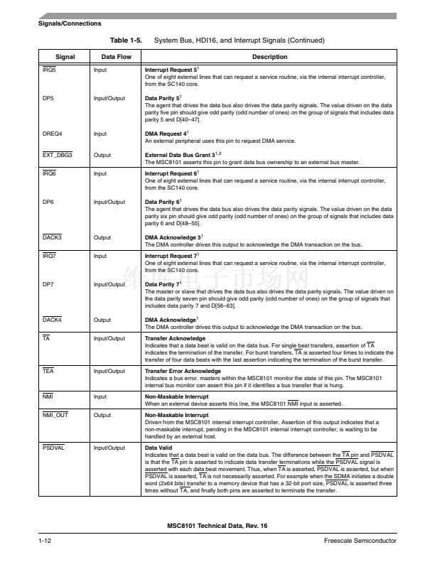
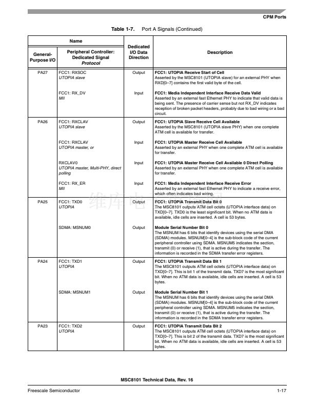
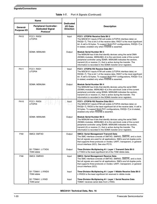
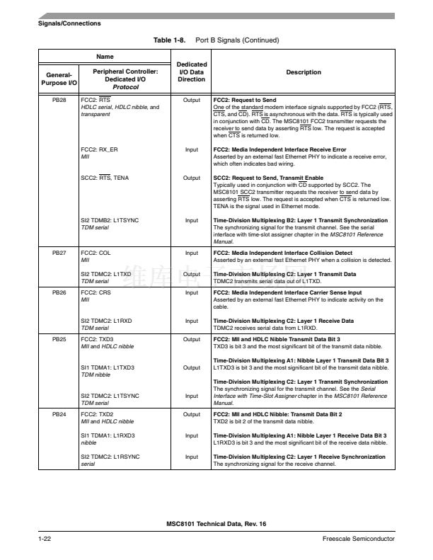
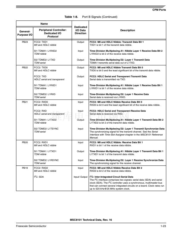
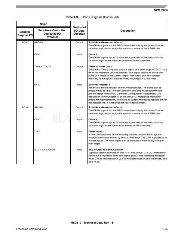
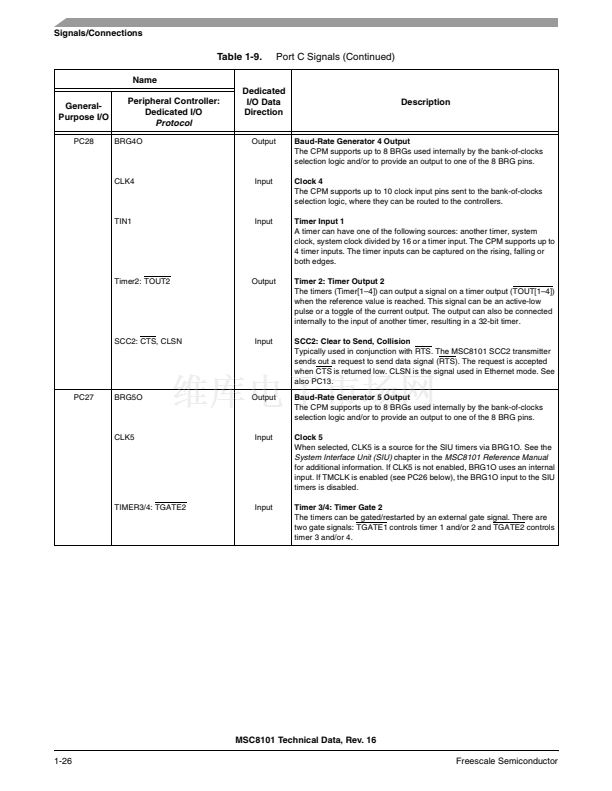
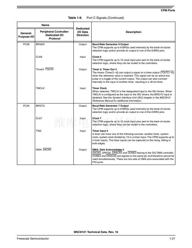
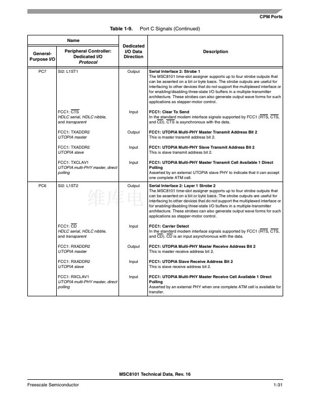
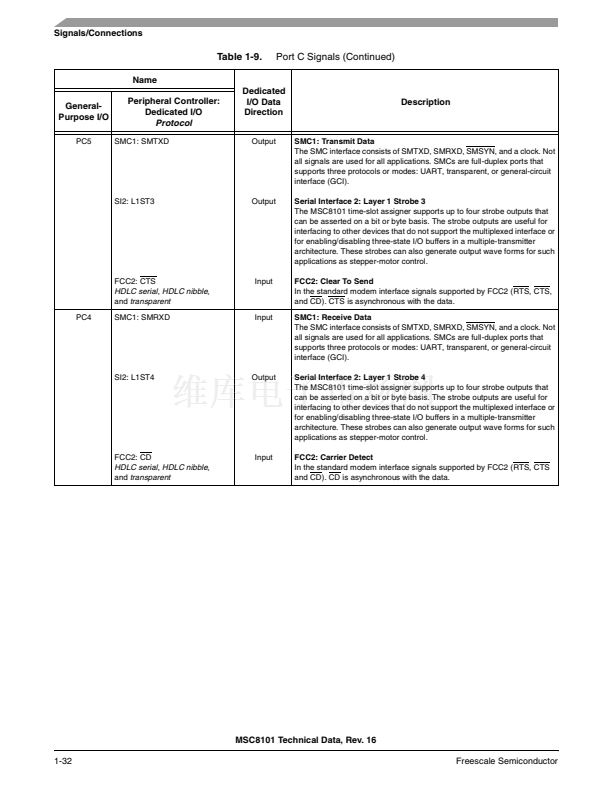
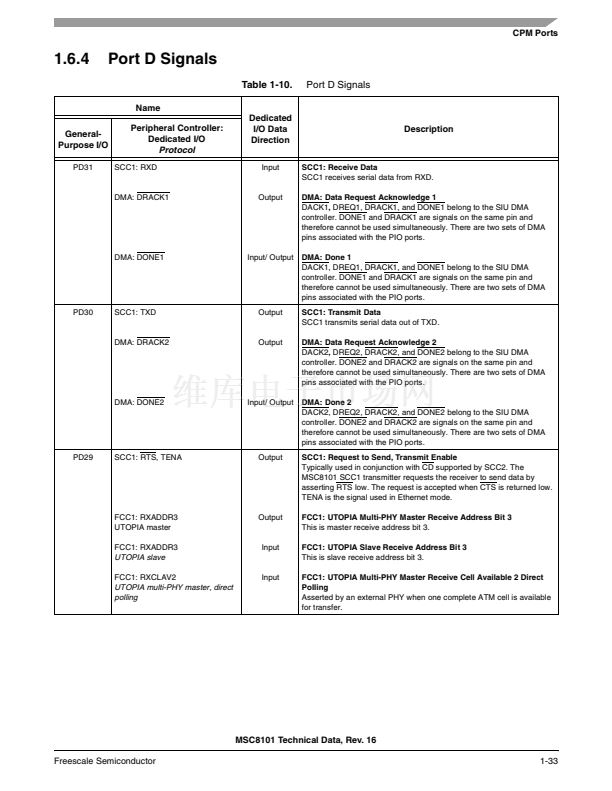
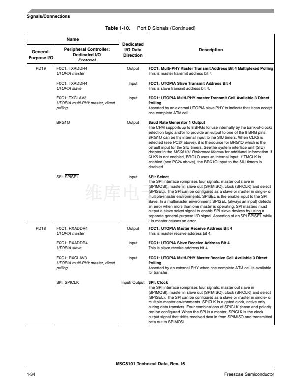
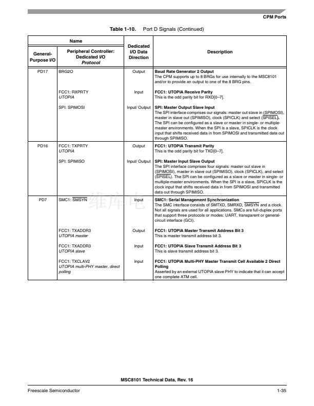
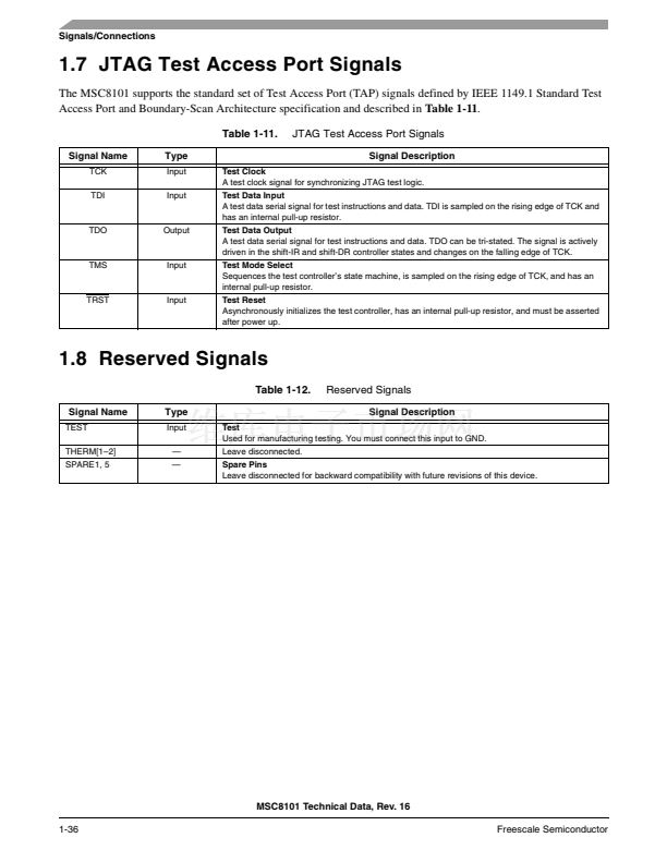
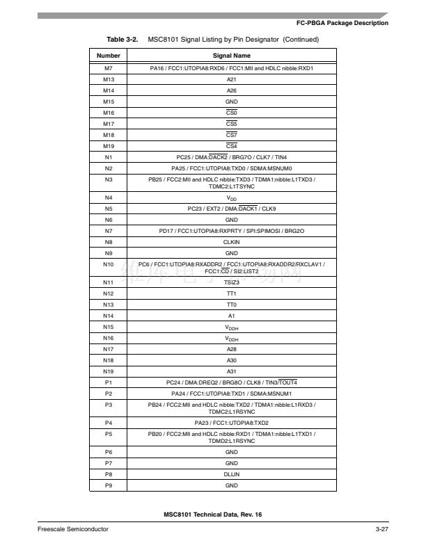
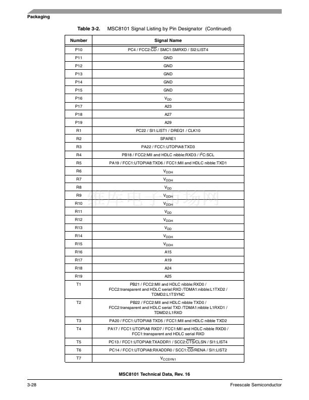
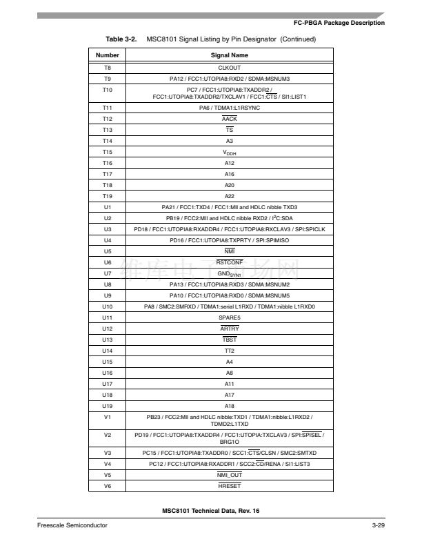
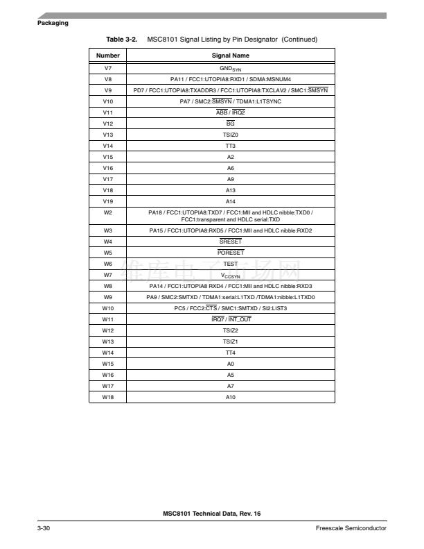
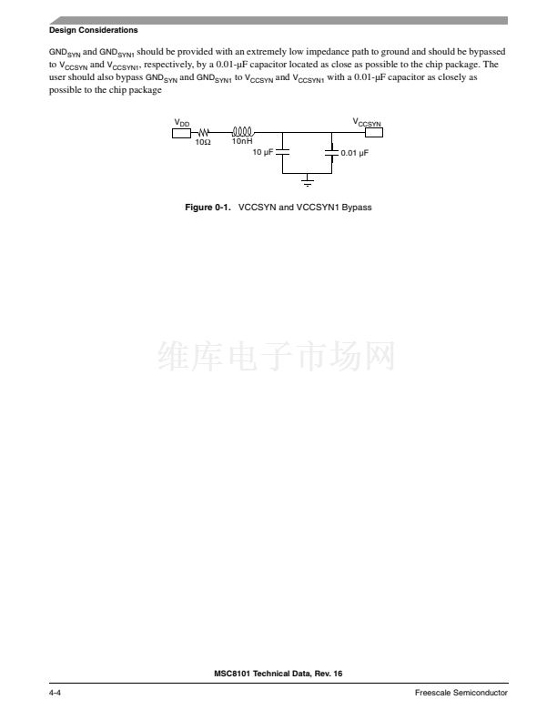
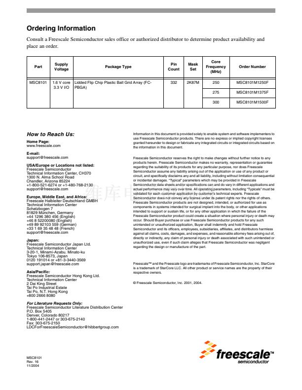
CPM Ports
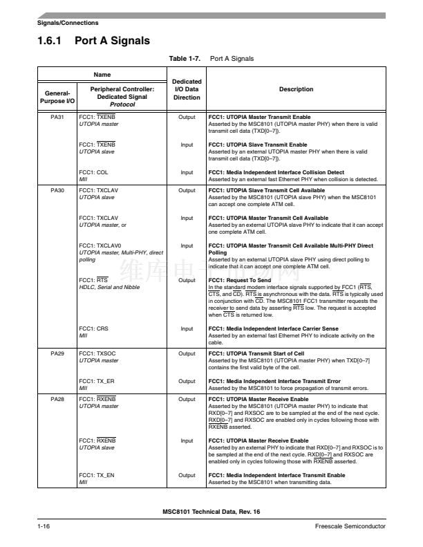
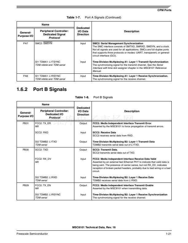
Table 1-7.
Name
General-
Purpose I/O
PA27
Port A Signals (Continued)
Peripheral Controller:
Dedicated Signal
Protocol
FCC1: RXSOC
UTOPIA slave
Dedicated
I/O Data
Direction
Output
Description
FCC1: UTOPIA Receive Start of Cell
Asserted by the MSC8101 (UTOPIA slave) for an external PHY when
RXD[0鈥?] contains the first valid byte of the cell.
FCC1: Media Independent Interface Receive Data Valid
Asserted by an external fast Ethernet PHY to indicate that valid data is
being sent. The presence of carrier sense but not RX_DV indicates
reception of broken packet headers, probably due to bad wiring or a bad
circuit.
FCC1: UTOPIA Slave Receive Cell Available
Asserted by the MSC8101 (UTOPIA slave PHY) when one complete
ATM cell is available for transfer.
FCC1: UTOPIA Master Receive Cell Available
Asserted by an external PHY when one complete ATM cell is available
for transfer.
FCC1: UTOPIA Master Receive Cell Available 0 Direct Polling
Asserted by an external PHY when one complete ATM cell is available
for transfer.
FCC1: Media Independent Interface Receive Error
Asserted by an external fast Ethernet PHY to indicate a receive error,
which often indicates bad wiring.
FCC1: UTOPIA Transmit Data Bit 0
The MSC8101 outputs ATM cell octets (UTOPIA interface data) on
TXD[0鈥?]. TXD0 is the least significant bit. When no ATM data is
available, idle cells are inserted. A cell is 53 bytes.
Module Serial Number Bit 0
The MSNUM has 6 bits that identify devices using the serial DMA
(SDMA) modules. MSNUM[0鈥?] is the sub-block code of the current
peripheral controller using SDMA. MSNUM5 indicates the section,
transmit (0) or receive (1), that is active during the transfer. The
information is recorded in the SDMA transfer error registers.
FCC1: UTOPIA Transmit Data Bit 1
The MSC8101 outputs ATM cell octets (UTOPIA interface data) on
TXD[0鈥?]. This is bit 1 of the transmit data. TXD7 is the most significant
bit. When no ATM data is available, idle cells are inserted. A cell is 53
bytes.
Module Serial Number Bit 1
The MSNUM has 6 bits that identify devices using the serial DMA
(SDMA) modules. MSNUM[0鈥?] is the sub-block code of the current
peripheral controller using SDMA. MSNUM5 indicates the section,
transmit (0) or receive (1), that is active during the transfer. The
information is recorded in the SDMA transfer error registers.
FCC1: UTOPIA Transmit Data Bit 2
The MSC8101 outputs ATM cell octets (UTOPIA interface data) on
TXD[0鈥?]. This is bit 2 of the transmit data. TXD7 is the most significant
bit. When no ATM data is available, idle cells are inserted. A cell is 53
bytes.
FCC1: RX_DV
MII
Input
PA26
FCC1: RXCLAV
UTOPIA slave
Output
FCC1: RXCLAV
UTOPIA master, or
Input
RXCLAV0
UTOPIA master, Multi-PHY, direct
polling
FCC1: RX_ER
MII
PA25
FCC1: TXD0
UTOPIA
Input
Input
Output
SDMA: MSNUM0
Output
PA24
FCC1: TXD1
UTOPIA
Output
SDMA: MSNUM1
Output
PA23
FCC1: TXD2
UTOPIA
Output
MSC8101 Technical Data, Rev. 16
Freescale Semiconductor
1-17


 1
1
 2
2
 3
3
 4
4
 5
5
 6
6
 7
7
 8
8
 9
9
 10
10
 11
11
 12
12
 13
13
 14
14
 15
15
 16
16
 17
17
 18
18
 19
19
 20
20
 21
21
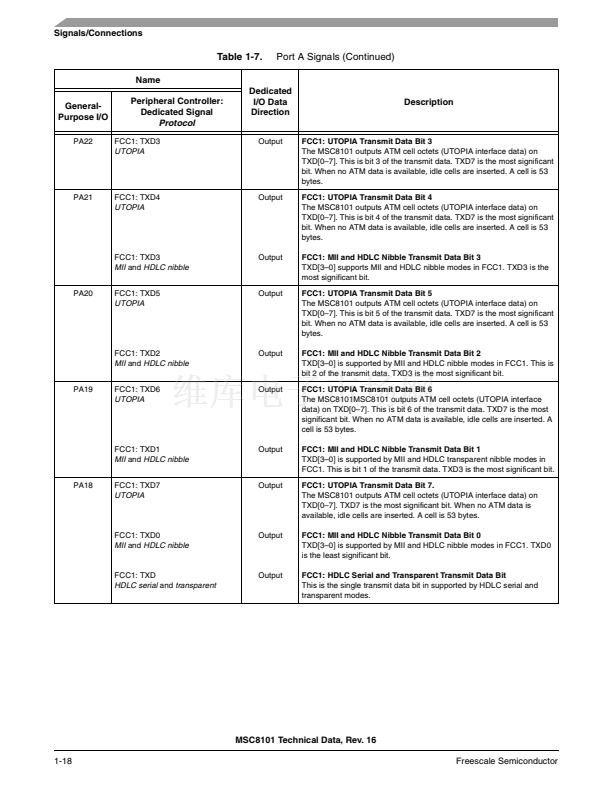 22
22
 23
23
 24
24
 25
25
 26
26
 27
27
 28
28
 29
29
 30
30
 31
31
 32
32
 33
33
 34
34
 35
35
 36
36
 37
37
 38
38
 39
39
 40
40
 41
41
 42
42
 43
43
 44
44
 45
45
 46
46
 47
47
 48
48
 49
49
 50
50
 51
51
 52
52
 53
53
 54
54
 55
55
 56
56
 57
57
 58
58
 59
59
 60
60
 61
61
 62
62
 63
63
 64
64
 65
65
 66
66
 67
67
 68
68
 69
69
 70
70
 71
71
 72
72
 73
73
 74
74
 75
75
 76
76
 77
77
 78
78
 79
79
 80
80
 81
81
 82
82
 83
83
 84
84
 85
85
 86
86
 87
87
 88
88
 89
89
 90
90
 91
91
 92
92
 93
93
 94
94
 95
95
 96
96
 97
97
 98
98
 99
99
 100
100
 101
101
 102
102
 103
103
 104
104
