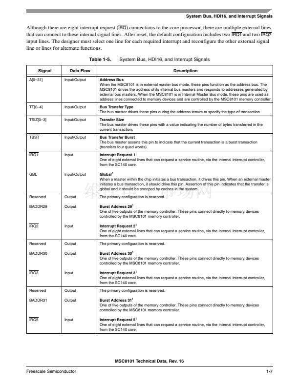
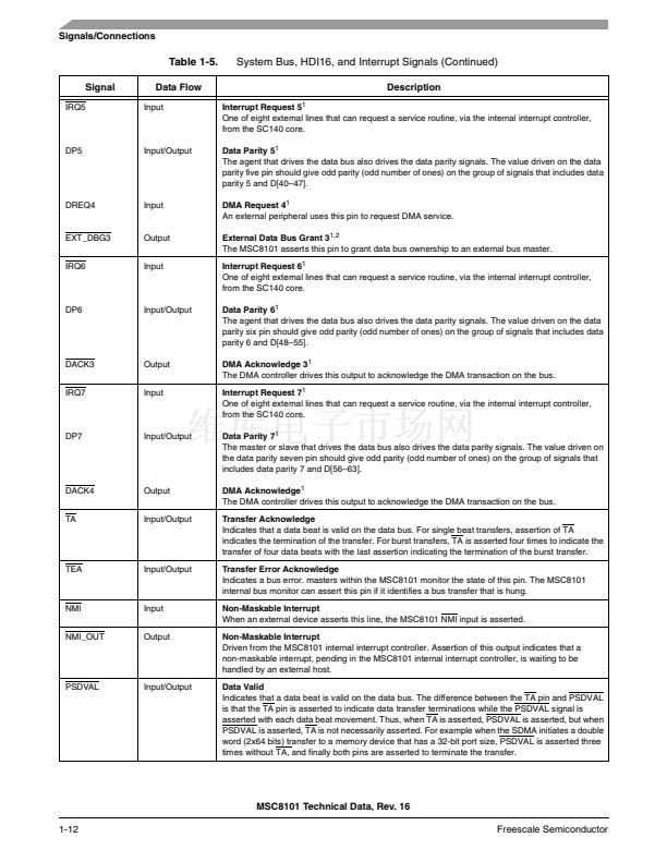
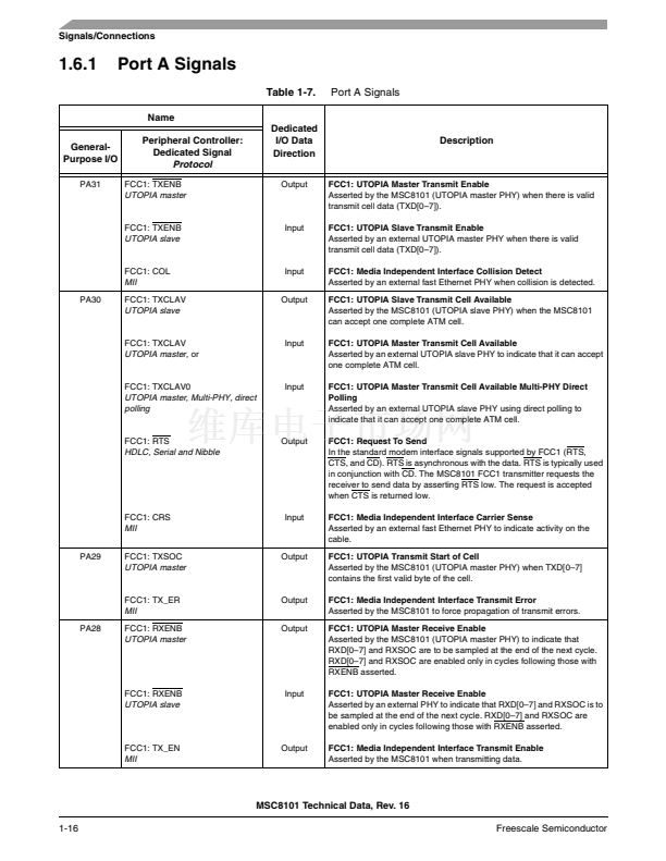
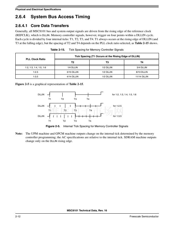
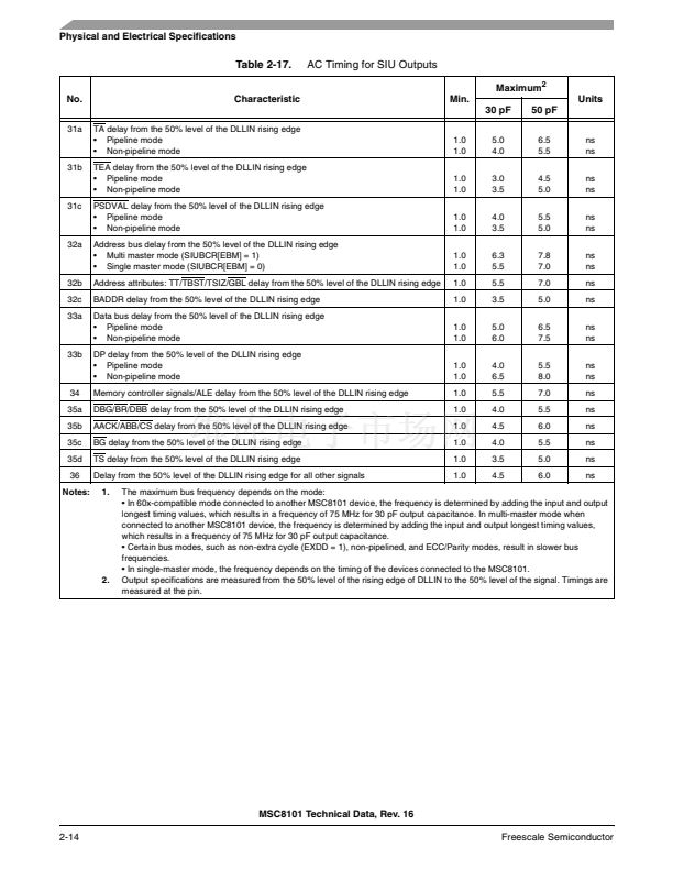
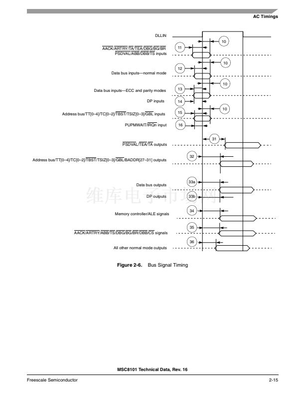
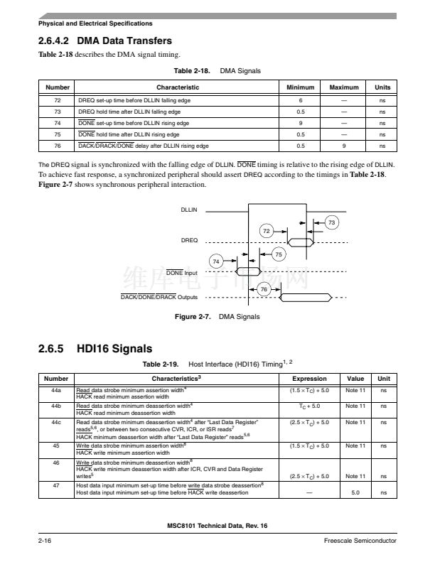
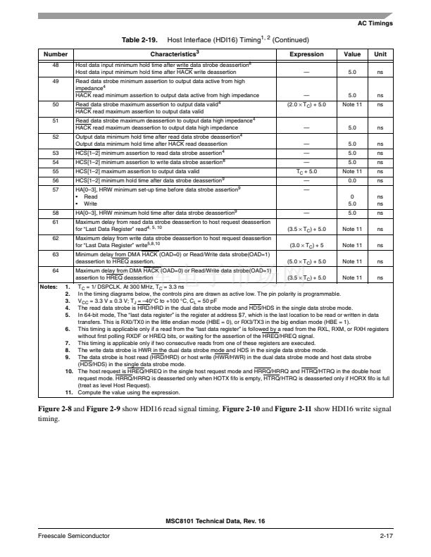
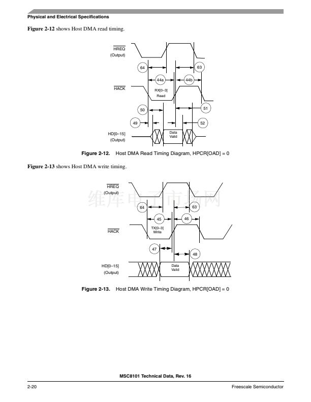
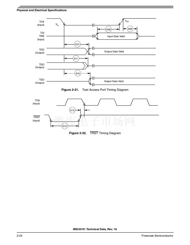
AC Timings
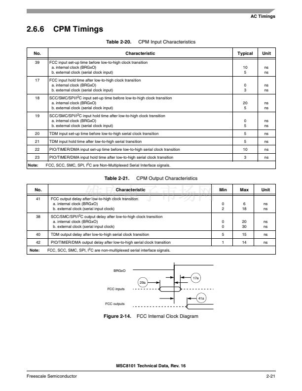
2.6.6
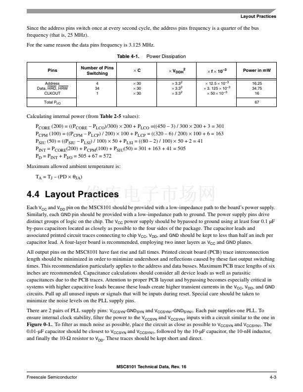
No.
39
CPM Timings
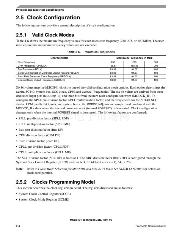
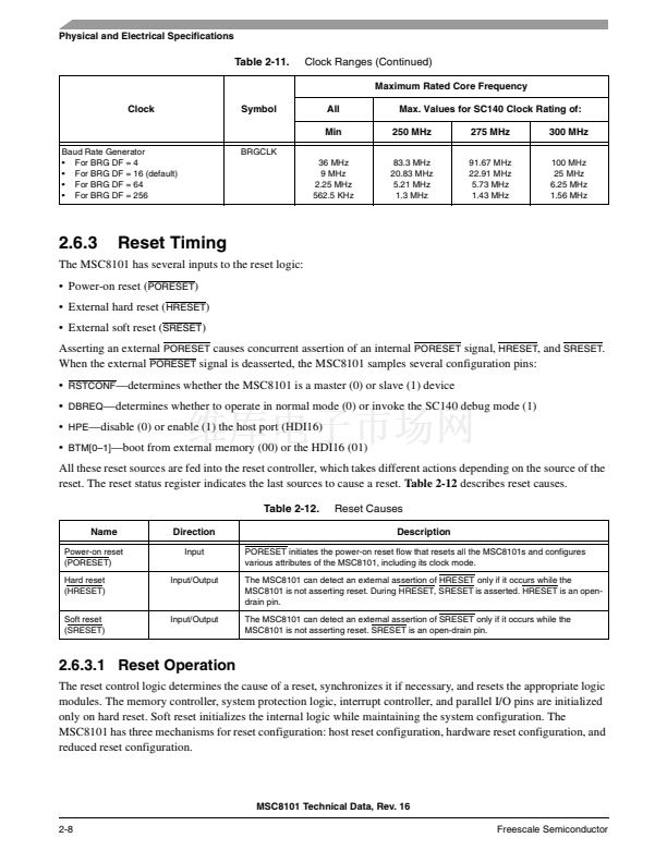
Table 2-20.
CPM Input Characteristics
Typical
10
5
0
3
20
5
0
5
5
5
10
3
Characteristic
FCC input set-up time before low-to-high clock transition
a. internal clock (BRGxO)
b. external clock (serial clock input)
FCC input hold time after low-to-high clock transition
a. internal clock (BRGxO)
b. external clock (serial clock input)
SCC/SMC/SPI/I
2
C input set-up time before low-to-high clock transition
a. internal clock (BRGxO)
b. external clock (serial clock input)
SCC/SMC/SPI/I
2
C input hold time after low-to-high clock transition
a. internal clock (BRGxO)
b. external clock (serial clock input)
TDM input set-up time before low-to-high serial clock transition
TDM input hold time after low-to-high serial transition
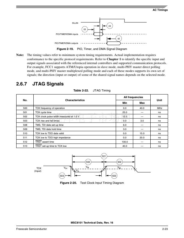
PIO/TIMER/DMA input set-up time before low-to-high serial clock transition
PIO/TIMER/DMA input hold time after low-to-high serial clock transition
FCC, SCC, SMC, SPI, I
2
C are Non-Multiplexed Serial Interface signals.
Unit
ns
ns
ns
ns
ns
ns
ns
ns
ns
ns
ns
ns
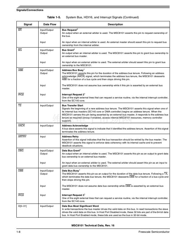
17
18
19
20
21
22
23
Note:
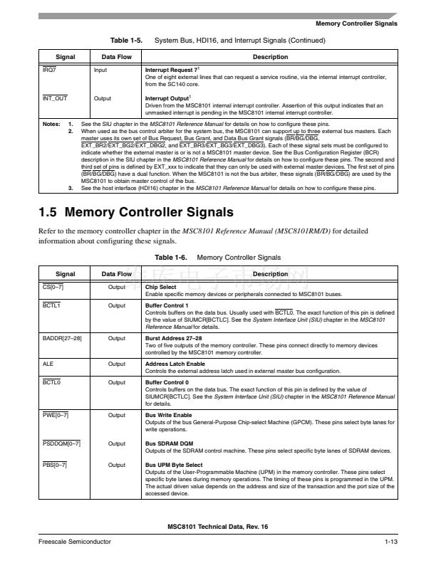
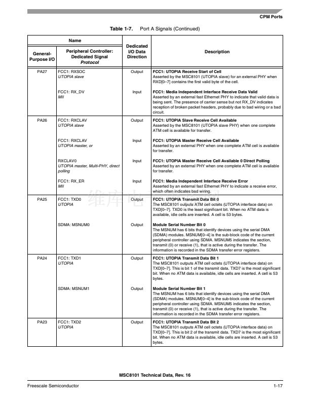
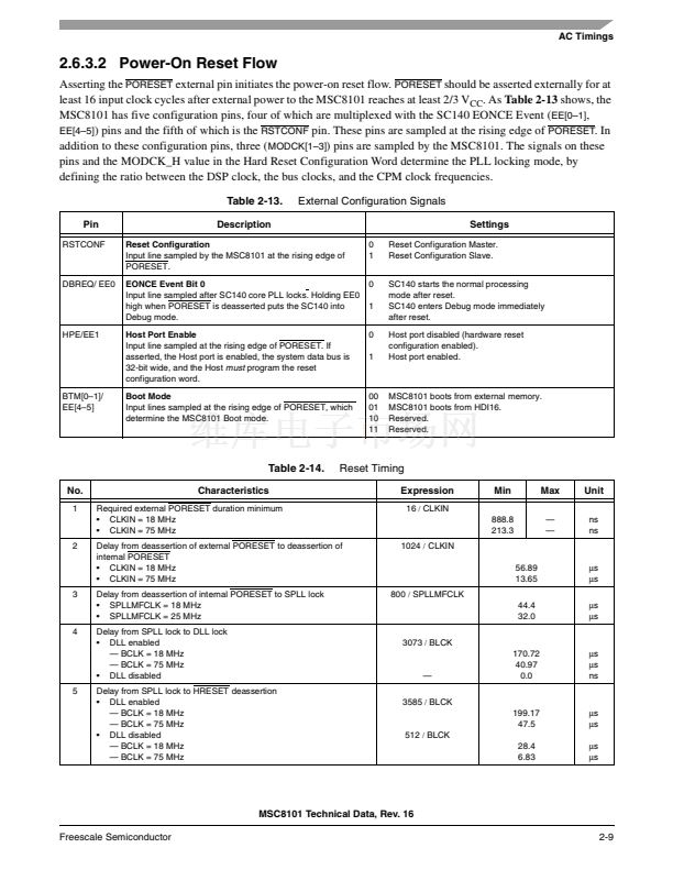
Table 2-21.
No.
41
CPM Output Characteristics
Min
0
2
0
0
5
1
Characteristic
FCC output delay after low-to-high clock transition
a. internal clock (BRGxO)
b. external clock (serial input clock)
SCC/SMC/SPI/I
2
C output delay after low-to-high clock transition
a. internal clock (BRGxO)
b. external clock (serial input clock)
TDM output delay after low-to-high serial clock transition
PIO/TIMER/DMA output delay after low-to-high serial clock transition
FCC, SCC, SMC, SPI, I
2
C are non-multiplexed serial interface signals.
Max
6
18
20
30
15
14
Unit
ns
ns
ns
ns
ns
ns
38
40
42
Note:
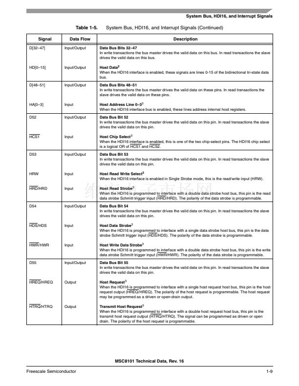
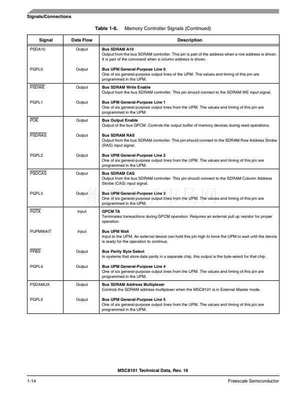
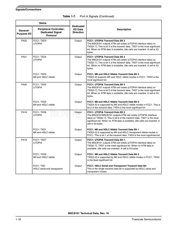
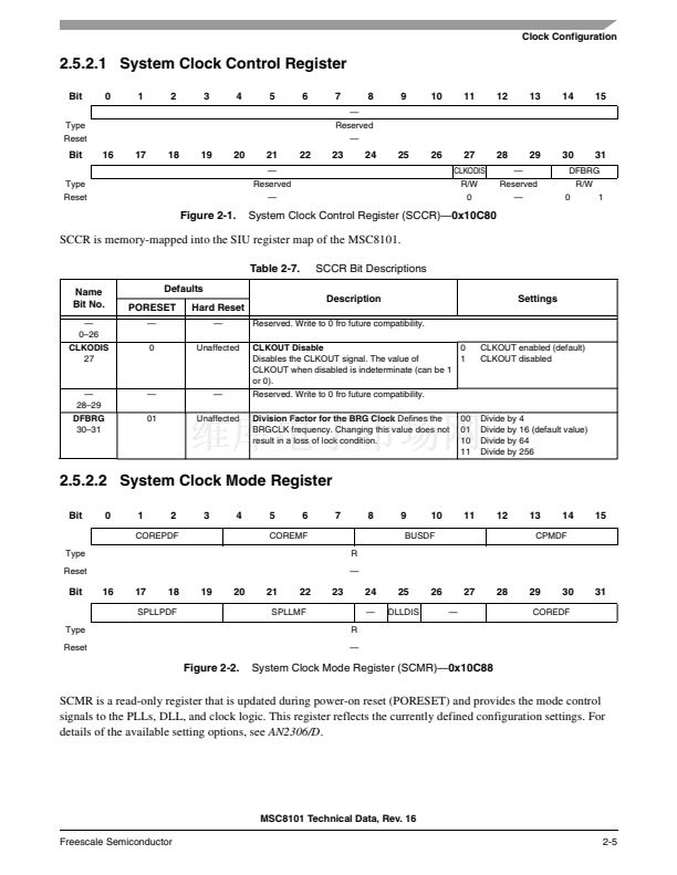
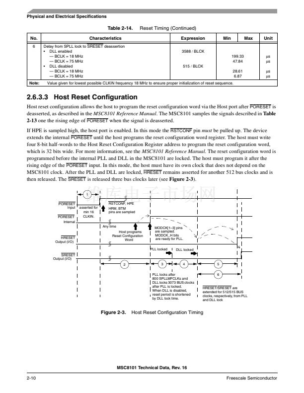
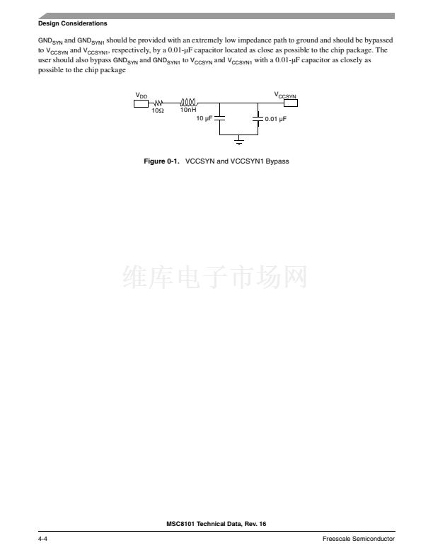
BRGxO
17a
29a
FCC inputs
41a
FCC outputs
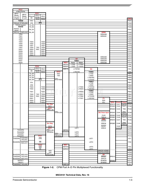
Figure 2-14.
FCC Internal Clock Diagram
MSC8101 Technical Data, Rev. 16
Freescale Semiconductor
2-21


 1
1
 2
2
 3
3
 4
4
 5
5
 6
6
 7
7
 8
8
 9
9
 10
10
 11
11
 12
12
 13
13
 14
14
 15
15
 16
16
 17
17
 18
18
 19
19
 20
20
 21
21
 22
22
 23
23
 24
24
 25
25
 26
26
 27
27
 28
28
 29
29
 30
30
 31
31
 32
32
 33
33
 34
34
 35
35
 36
36
 37
37
 38
38
 39
39
 40
40
 41
41
 42
42
 43
43
 44
44
 45
45
 46
46
 47
47
 48
48
 49
49
 50
50
 51
51
 52
52
 53
53
 54
54
 55
55
 56
56
 57
57
 58
58
 59
59
 60
60
 61
61
 62
62
 63
63
 64
64
 65
65
 66
66
 67
67
 68
68
 69
69
 70
70
 71
71
 72
72
 73
73
 74
74
 75
75
 76
76
 77
77
 78
78
 79
79
 80
80
 81
81
 82
82
 83
83
 84
84
 85
85
 86
86
 87
87
 88
88
 89
89
 90
90
 91
91
 92
92
 93
93
 94
94
 95
95
 96
96
 97
97
 98
98
 99
99
 100
100
 101
101
 102
102
 103
103
 104
104
