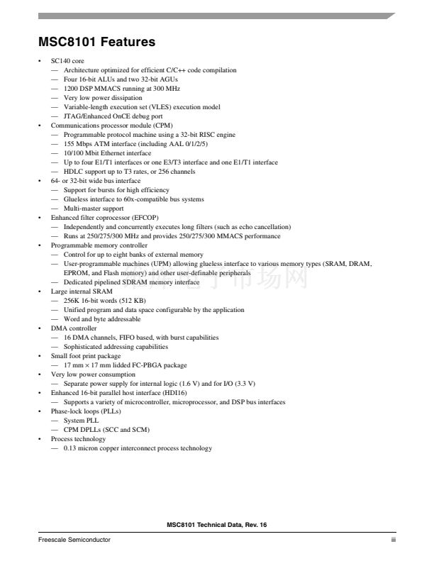
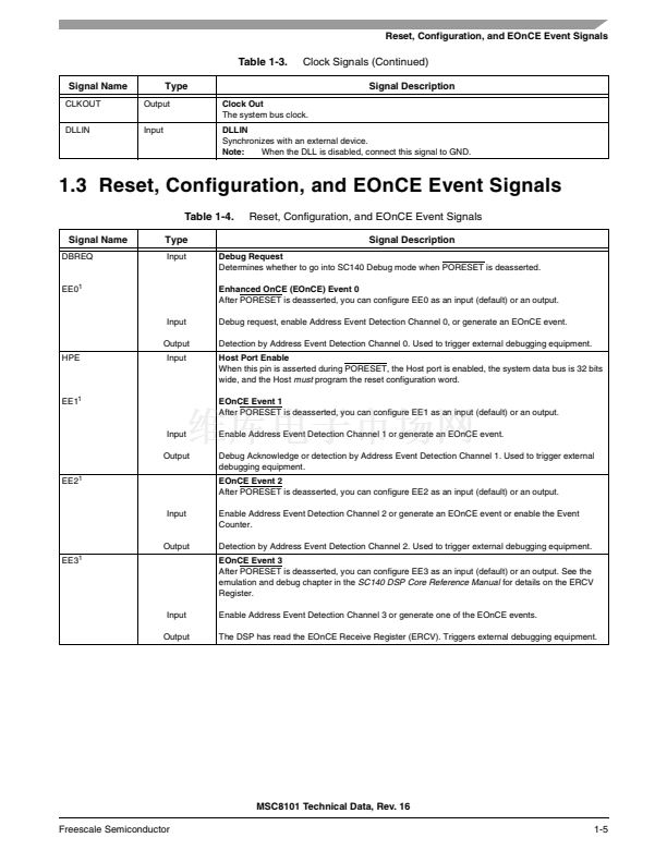
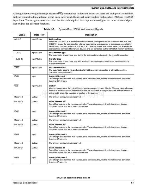
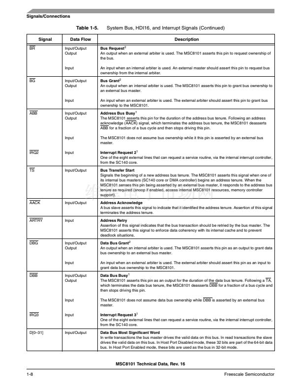
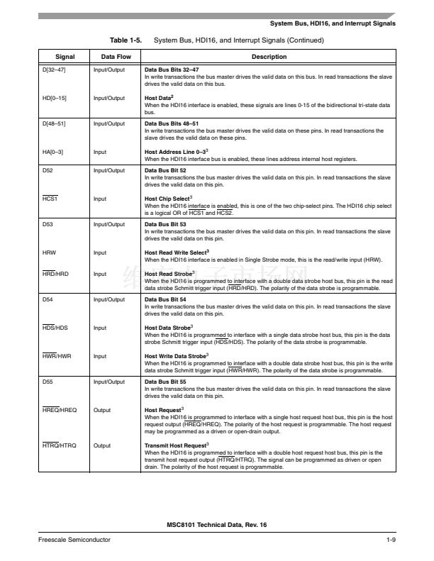
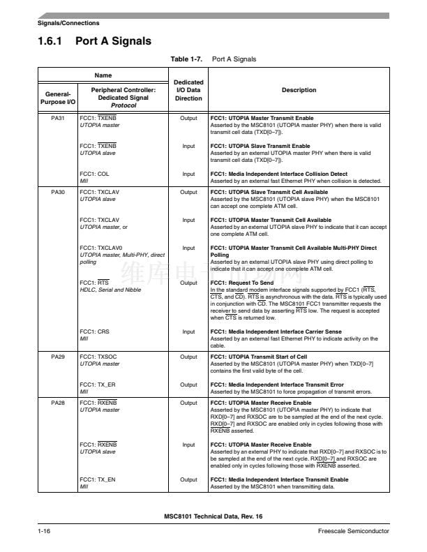
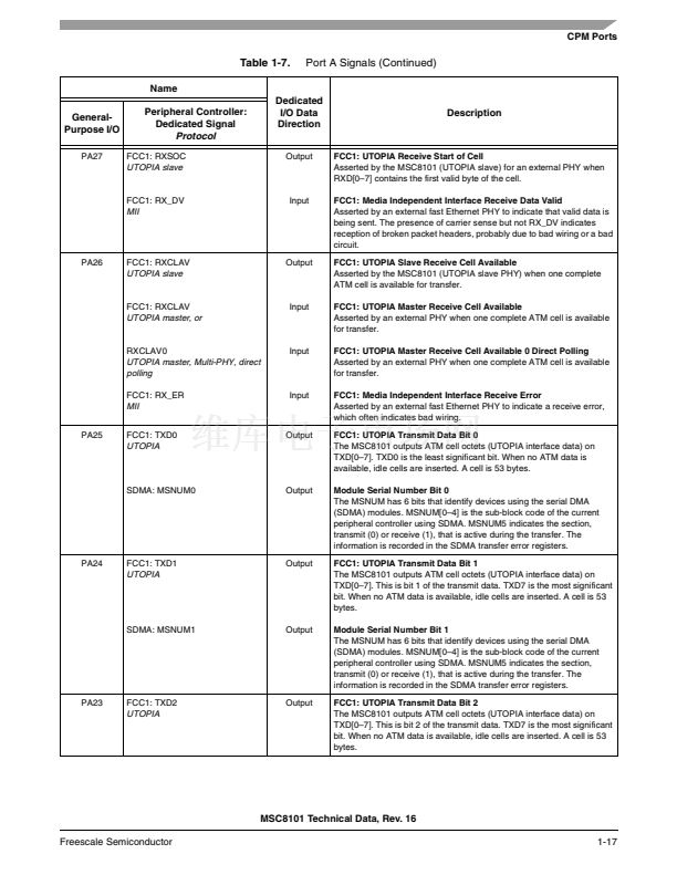
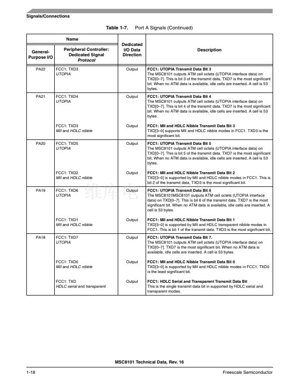
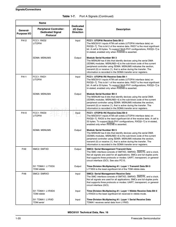
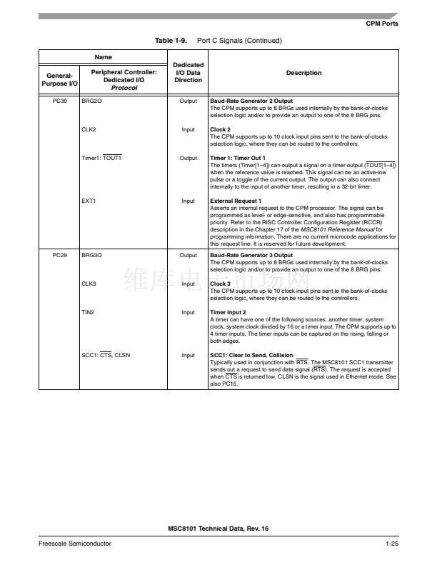
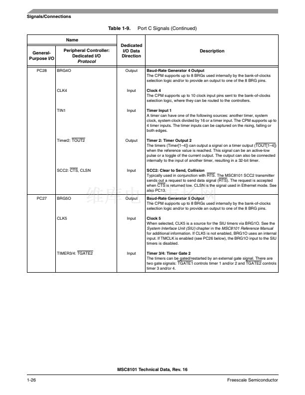
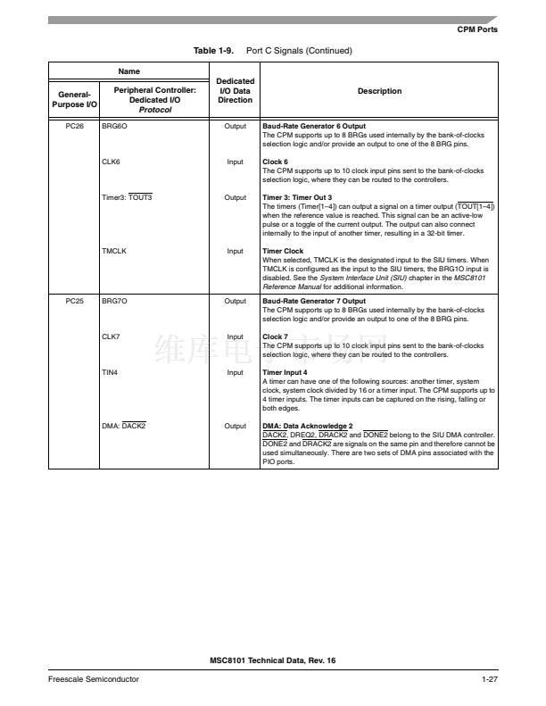
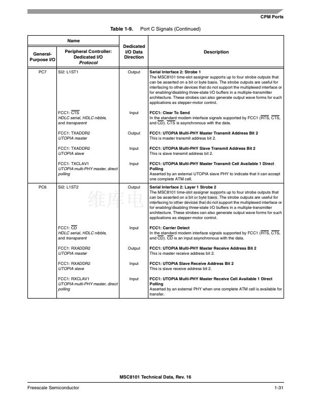
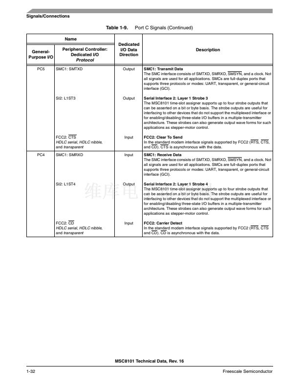
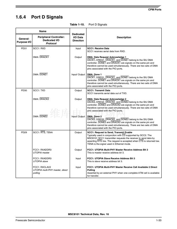
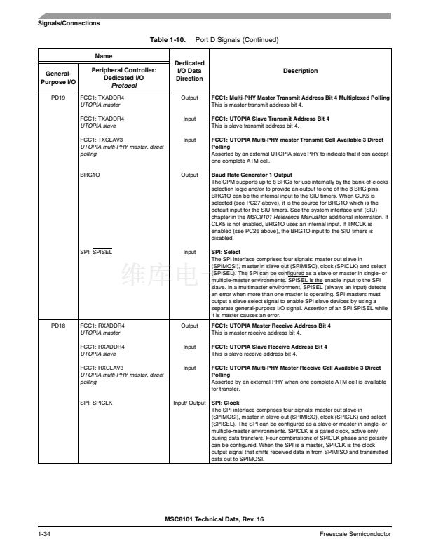
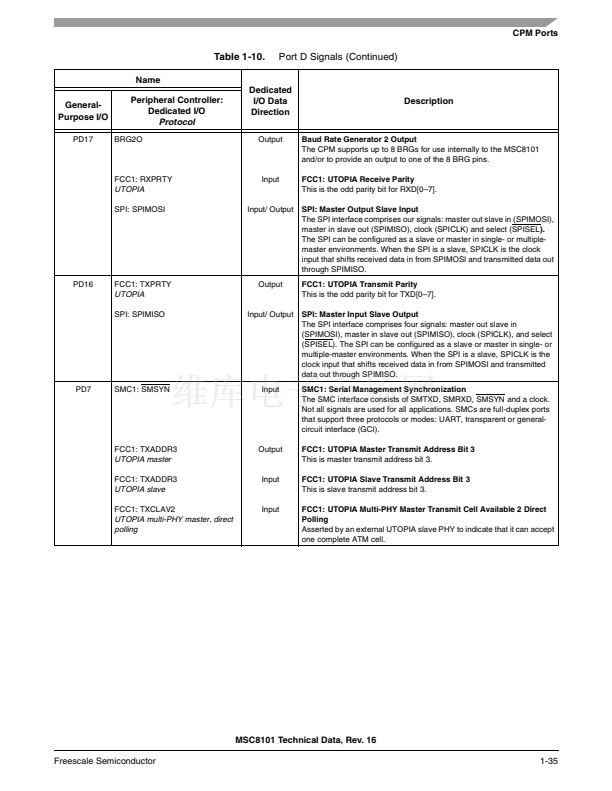
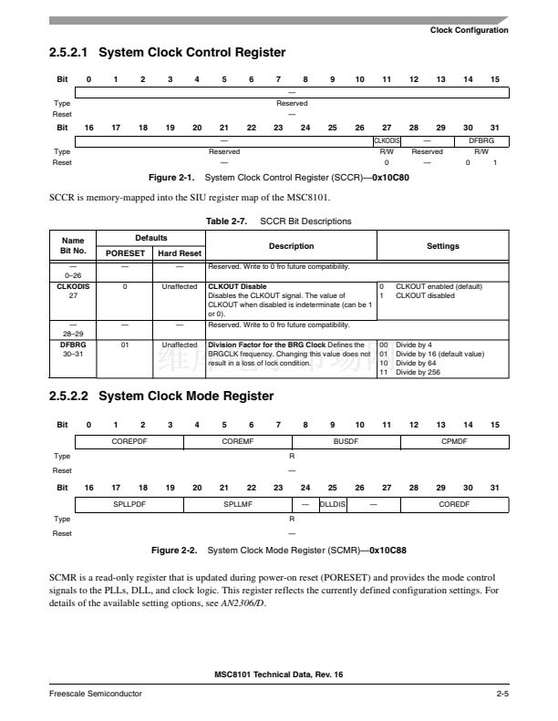
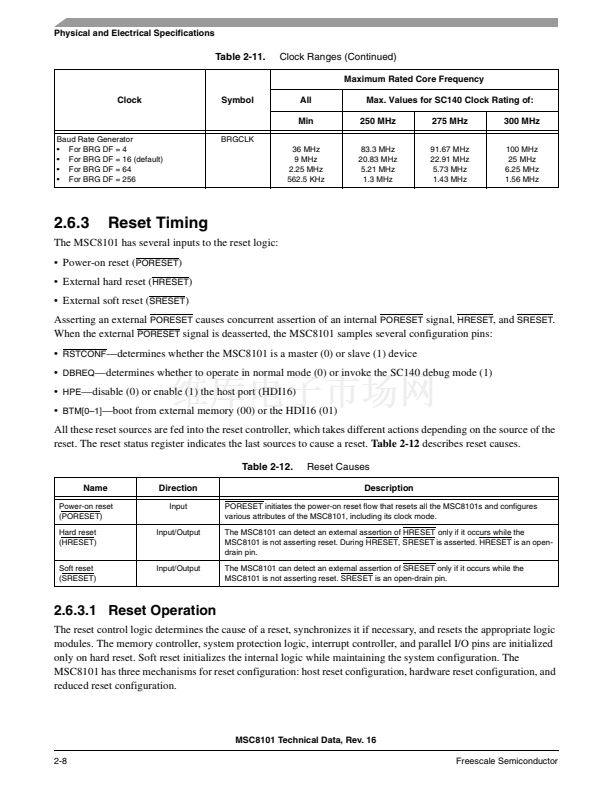
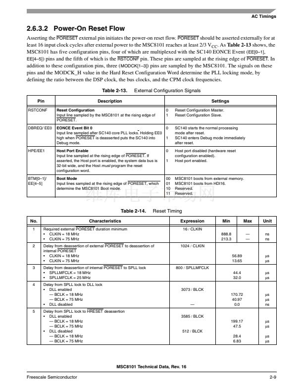
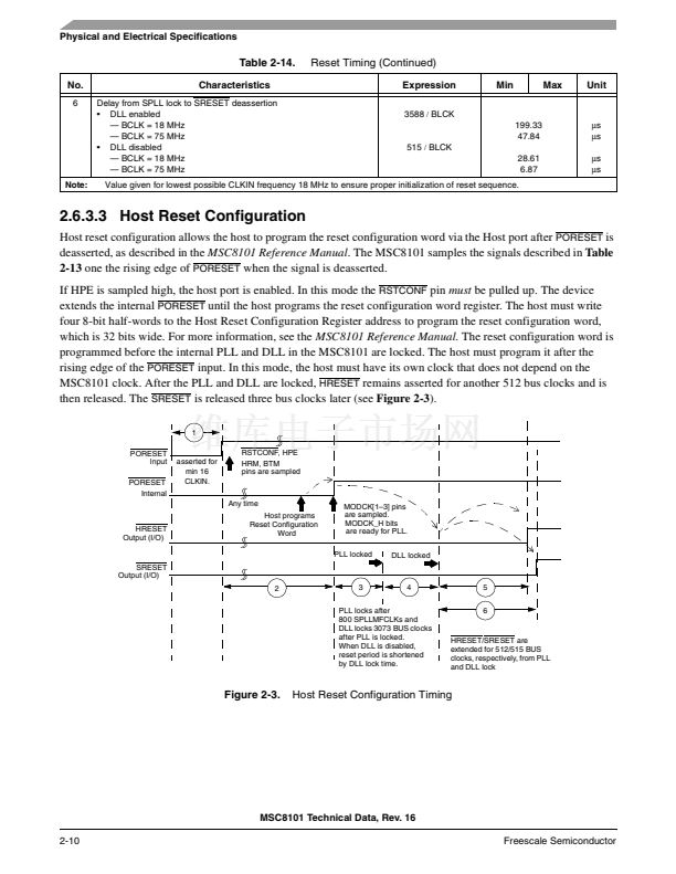
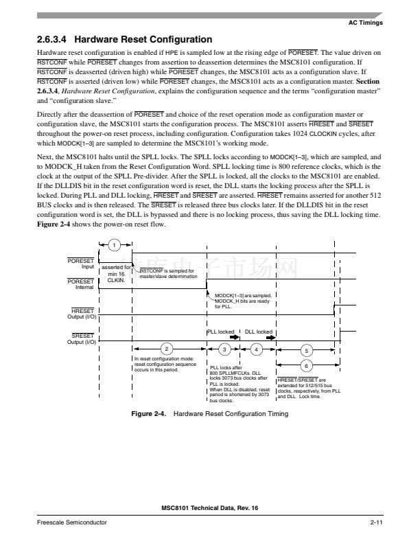
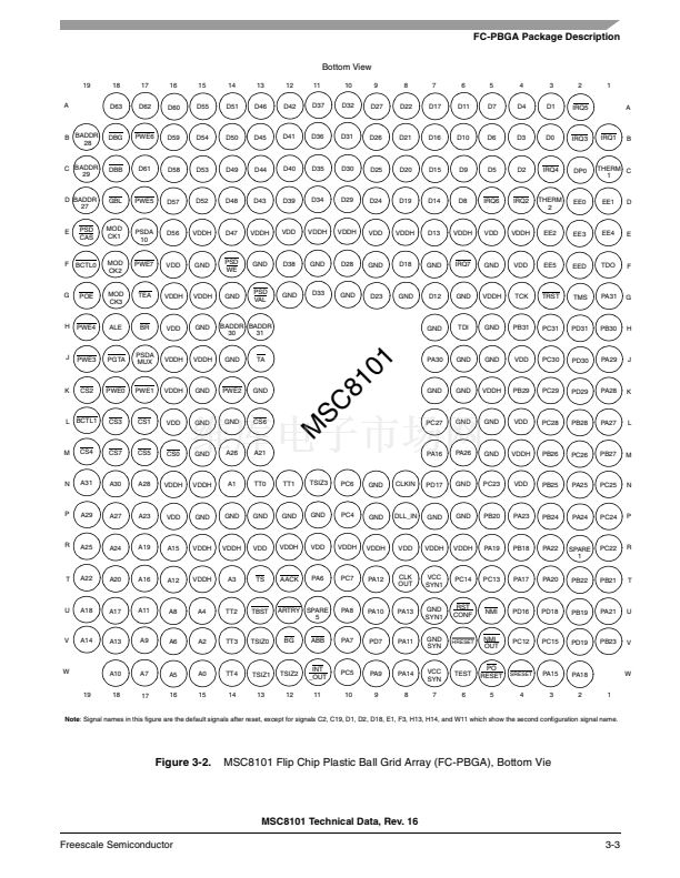
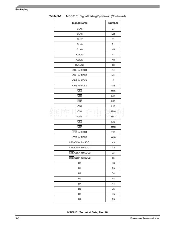
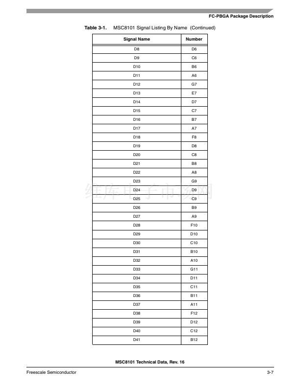
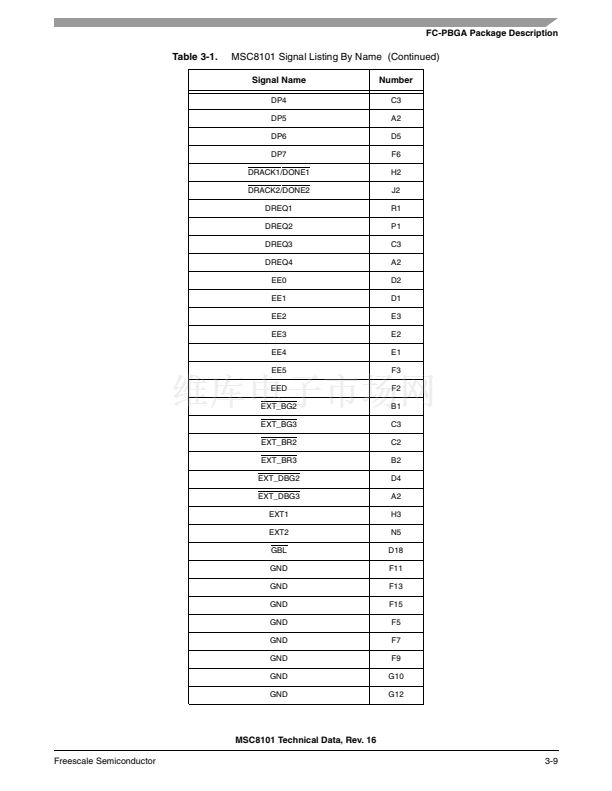
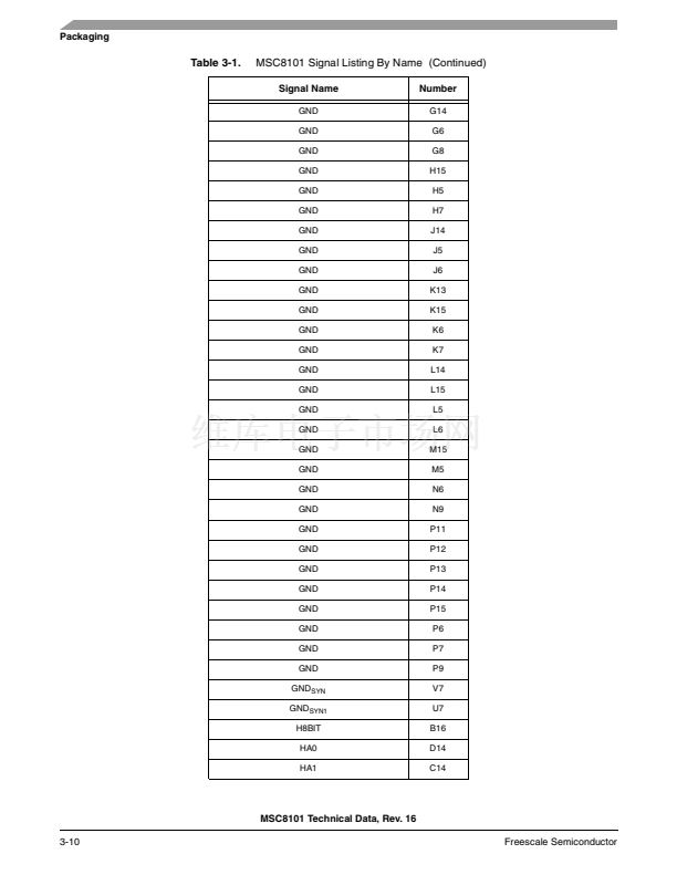
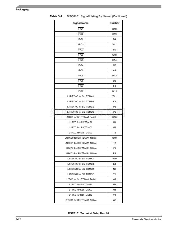
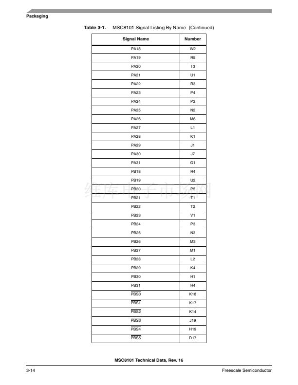
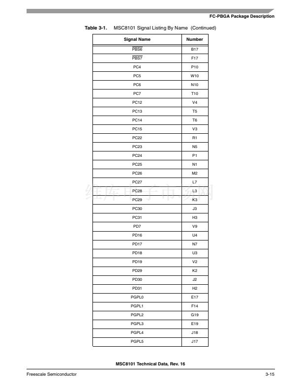
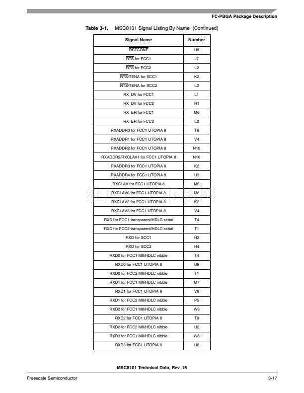
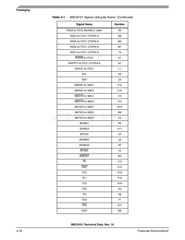
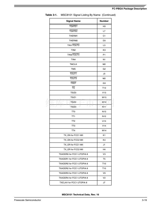
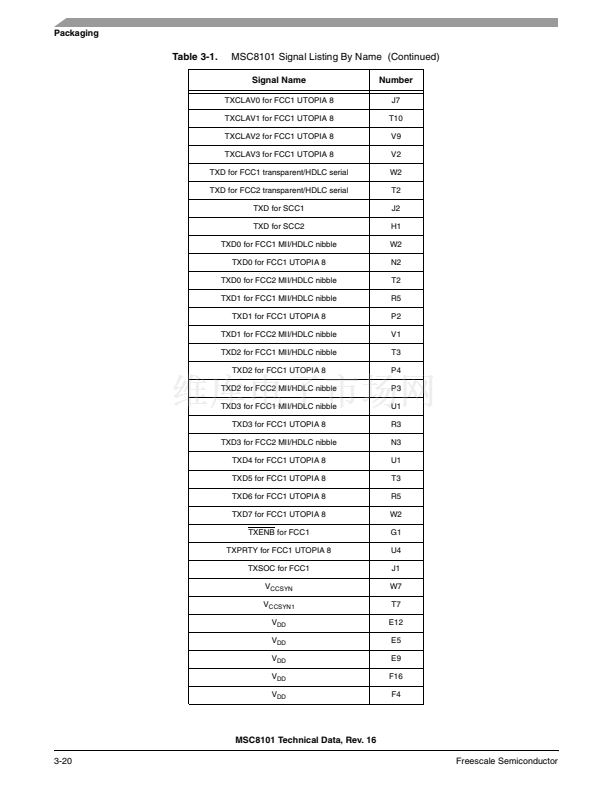
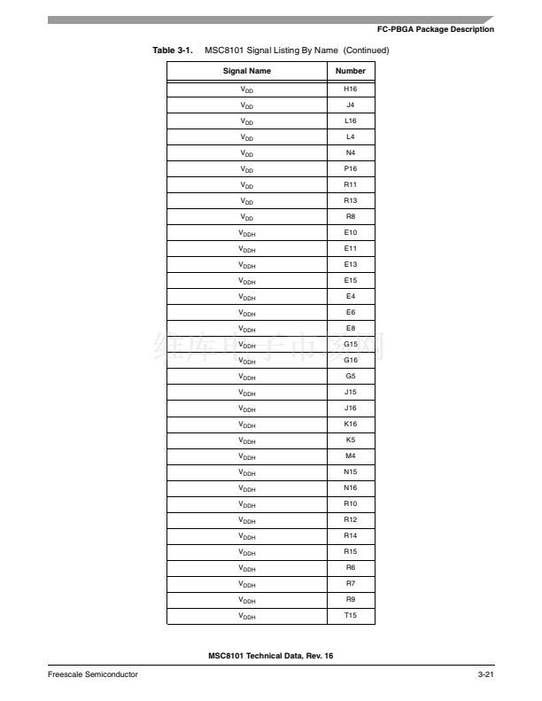
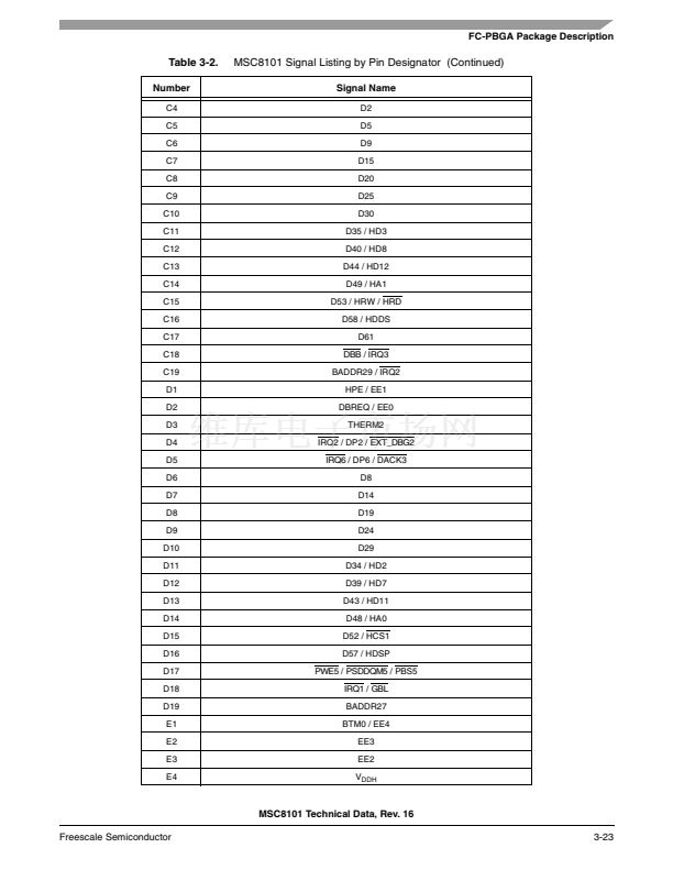
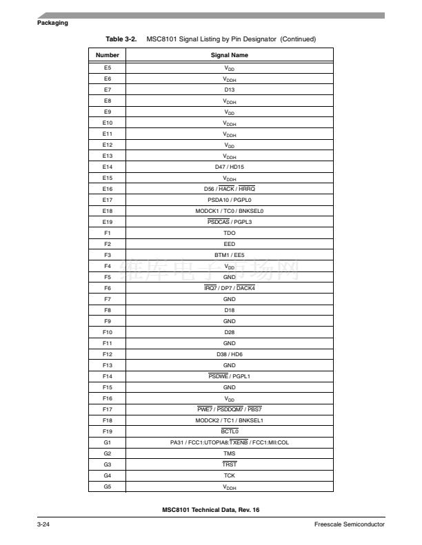
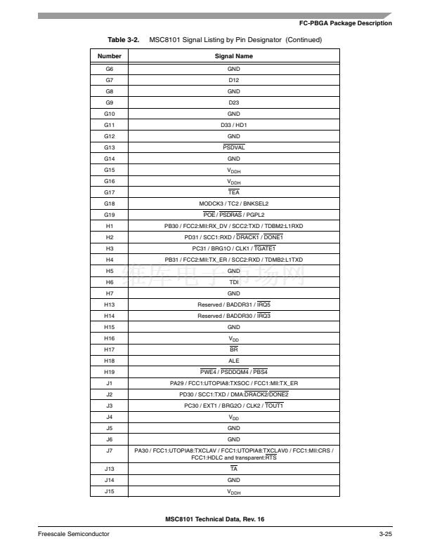
Physical and Electrical Specifications
2.6.4
System Bus Access Timing
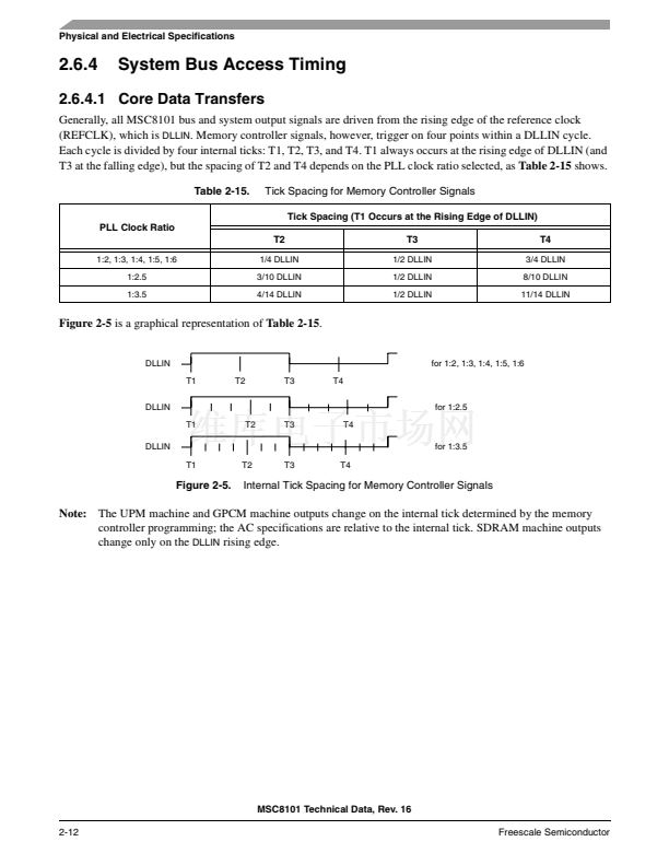
2.6.4.1 Core Data Transfers
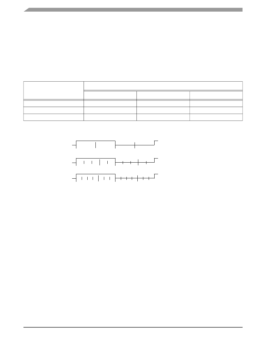
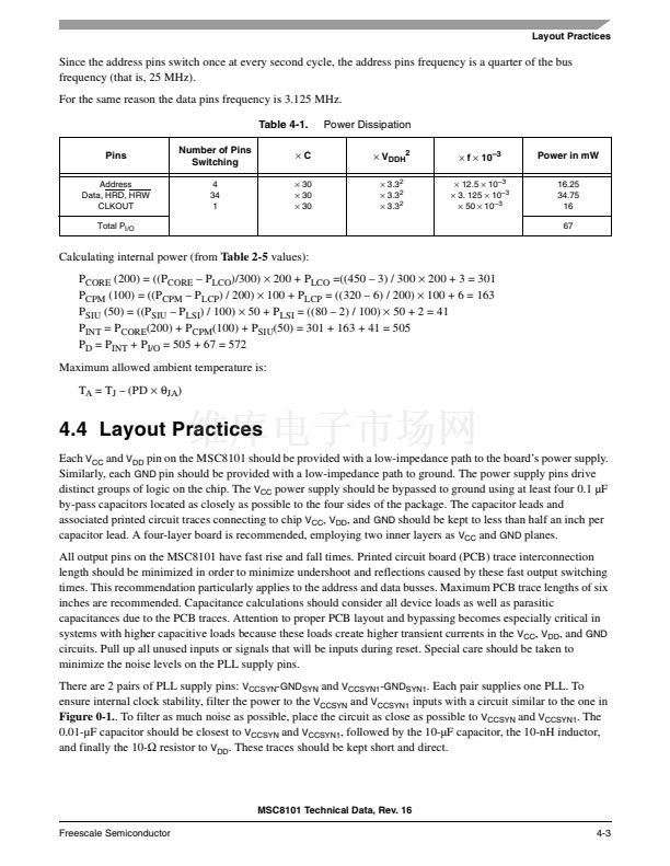
Generally, all MSC8101 bus and system output signals are driven from the rising edge of the reference clock
(REFCLK), which is
DLLIN
. Memory controller signals, however, trigger on four points within a DLLIN cycle.
Each cycle is divided by four internal ticks: T1, T2, T3, and T4. T1 always occurs at the rising edge of DLLIN (and
T3 at the falling edge), but the spacing of T2 and T4 depends on the PLL clock ratio selected, as
Table 2-15
shows.
Table 2-15.
Tick Spacing for Memory Controller Signals
Tick Spacing (T1 Occurs at the Rising Edge of DLLIN)
PLL Clock Ratio
T2
1:2, 1:3, 1:4, 1:5, 1:6
1:2.5
1:3.5
1/4 DLLIN
3/10 DLLIN
4/14 DLLIN
T3
1/2 DLLIN
1/2 DLLIN
1/2 DLLIN
T4
3/4 DLLIN
8/10 DLLIN
11/14 DLLIN
Figure 2-5
is a graphical representation of
Table 2-15.
DLLIN
T1
DLLIN
T1
DLLIN
T1
T2
T3
T4
T2
T3
T4
T2
T3
T4
for 1:2, 1:3, 1:4, 1:5, 1:6
for 1:2.5
for 1:3.5
Figure 2-5.
Internal Tick Spacing for Memory Controller Signals
Note:
The UPM machine and GPCM machine outputs change on the internal tick determined by the memory
controller programming; the AC specifications are relative to the internal tick. SDRAM machine outputs
change only on the
DLLIN
rising edge.
MSC8101 Technical Data, Rev. 16
2-12
Freescale Semiconductor


 1
1
 2
2
 3
3
 4
4
 5
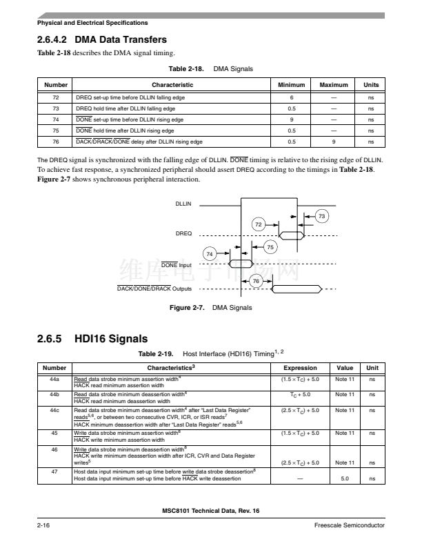
5
 6
6
 7
7
 8
8
 9
9
 10
10
 11
11
 12
12
 13
13
 14
14
 15
15
 16
16
 17
17
 18
18
 19
19
 20
20
 21
21
 22
22
 23
23
 24
24
 25
25
 26
26
 27
27
 28
28
 29
29
 30
30
 31
31
 32
32
 33
33
 34
34
 35
35
 36
36
 37
37
 38
38
 39
39
 40
40
 41
41
 42
42
 43
43
 44
44
 45
45
 46
46
 47
47
 48
48
 49
49
 50
50
 51
51
 52
52
 53
53
 54
54
 55
55
 56
56
 57
57
 58
58
 59
59
 60
60
 61
61
 62
62
 63
63
 64
64
 65
65
 66
66
 67
67
 68
68
 69
69
 70
70
 71
71
 72
72
 73
73
 74
74
 75
75
 76
76
 77
77
 78
78
 79
79
 80
80
 81
81
 82
82
 83
83
 84
84
 85
85
 86
86
 87
87
 88
88
 89
89
 90
90
 91
91
 92
92
 93
93
 94
94
 95
95
 96
96
 97
97
 98
98
 99
99
 100
100
 101
101
 102
102
 103
103
 104
104
