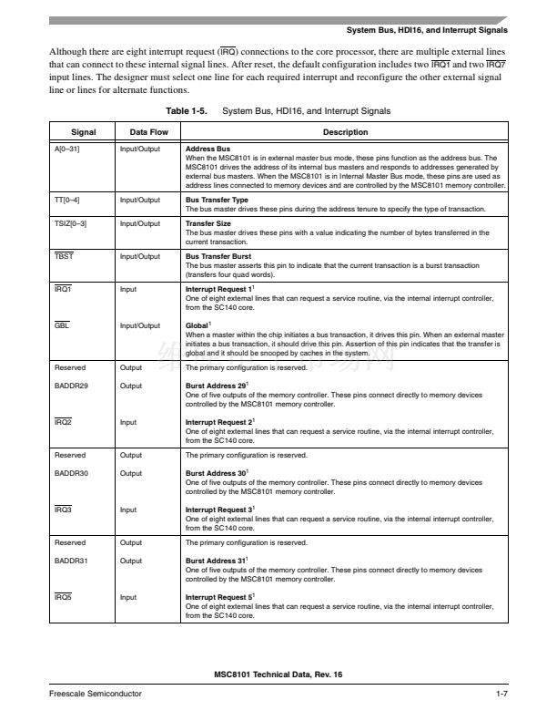
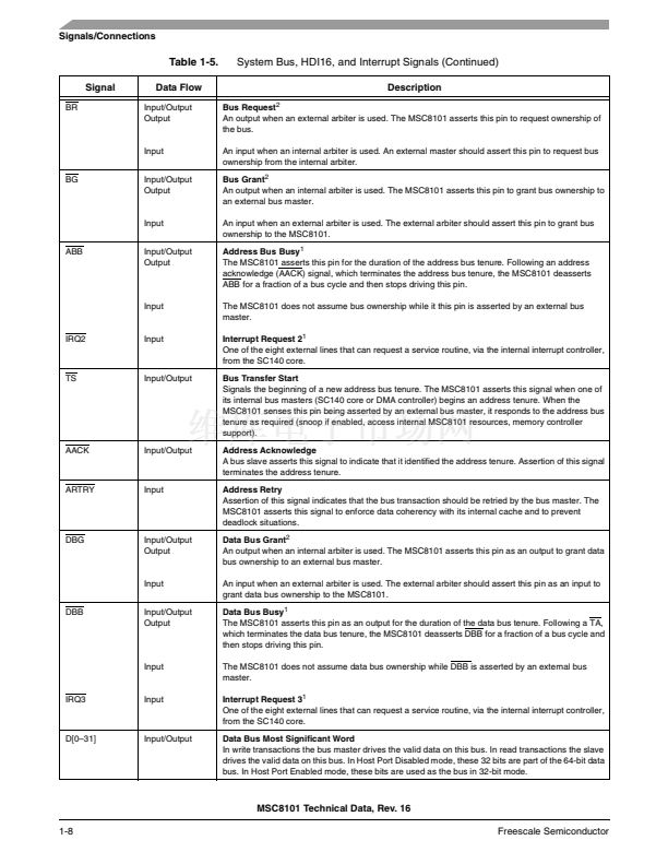
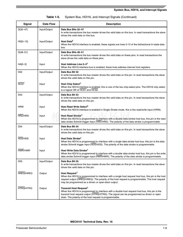
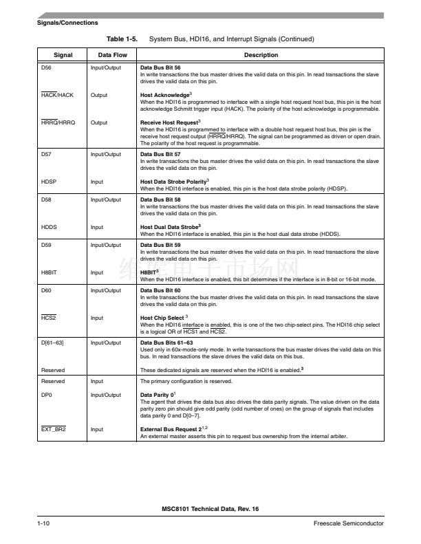
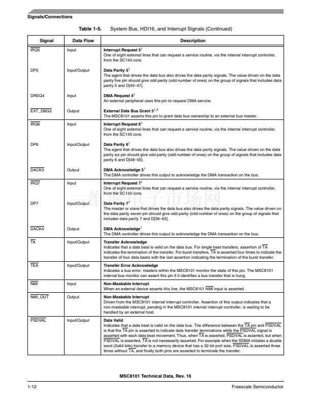
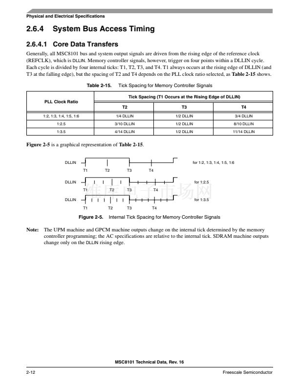
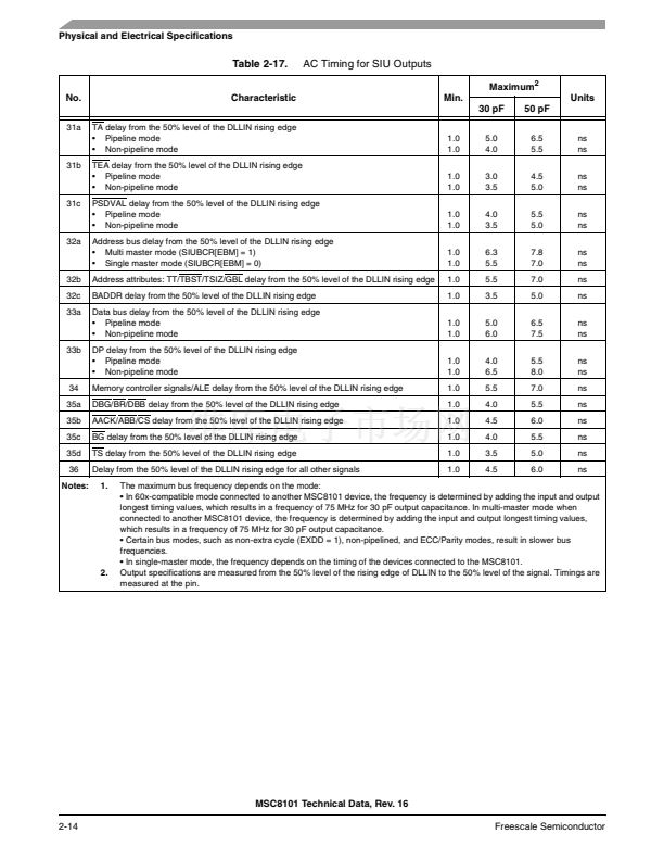
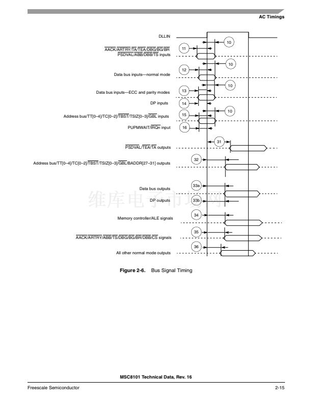
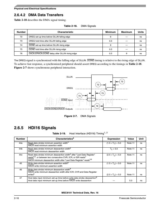
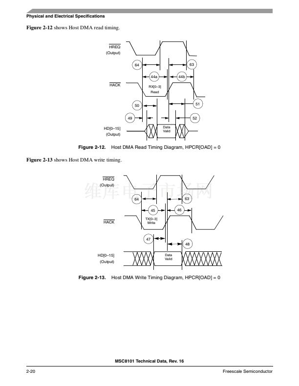
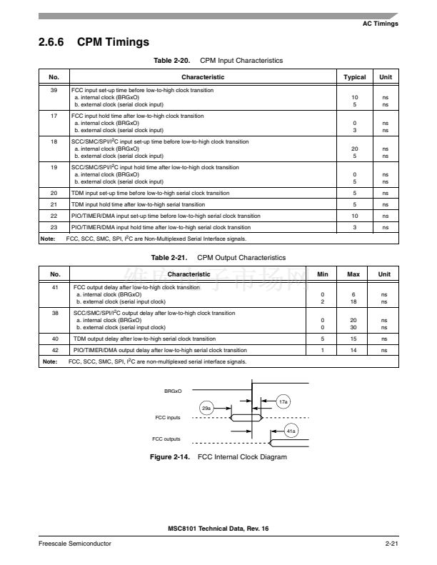
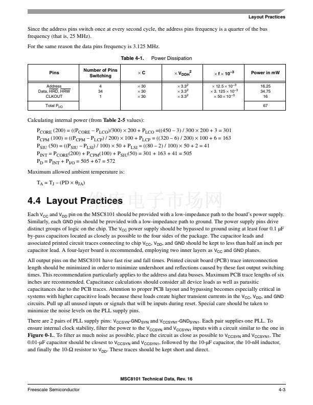
This chapter includes design and layout guidelines for manufacturing boards using the MSC8102.
鈥?/div>
胃
JA
)
Equation 1
where
胃
JA
= package thermal resistance
,
junction to ambient
,
掳C/W
P
D
= P
INT
+ P
I/O
in W
P
INT
= I
DD
脳
V
DD
in W鈥攃hip internal power
P
I/O
= power dissipation on output pins in W鈥攗ser determined
The user should set T
A
and P
D
such that T
J
does not exceed the maximum operating conditions. In case T
J
is too
high, the user should either lower the ambient temperature or the power dissipation of the chip.
T
A
= ambient temperature
掳C
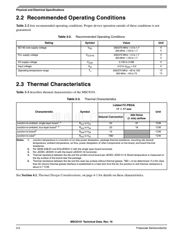
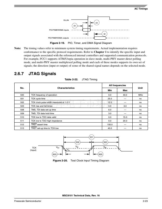
4.2 Electrical Design Considerations
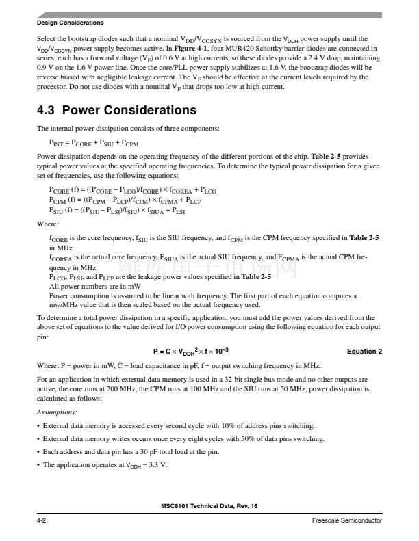
The input voltage must not exceed the I/O supply
V
DDH
by more than 2.5 V at any time, including during power-on
reset. In turn,
V
DDH
can exceed
V
DD
/
V
CCSYN
by more than 3.3 V during power-on reset, but for no more than 100 ms.
V
DDH
should not exceed
V
DD
/
V
CCSYN
by more than 2.1 V during normal operation.
V
DD
/
V
CCSYN
must not exceed
V
DDH
by more than 0.4 V at any time, including during power-on reset. Therefore the recommendation is to use
鈥渂ootstrap鈥?diodes between the power rails, as shown in
Figure 4-1.
I/O Power
MUR420
MUR420
MUR420
3.3 V (V
DDH
)
Core/PLL
Supply
MUR420
1.6 V (V
DD
/V
CCSYN
)
Figure 4-1.
Bootstrap Diodes for Power-Up Sequencing
MSC8101 Technical Data, Rev. 16
Freescale Semiconductor
4-1


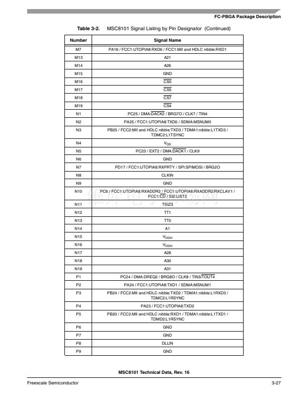
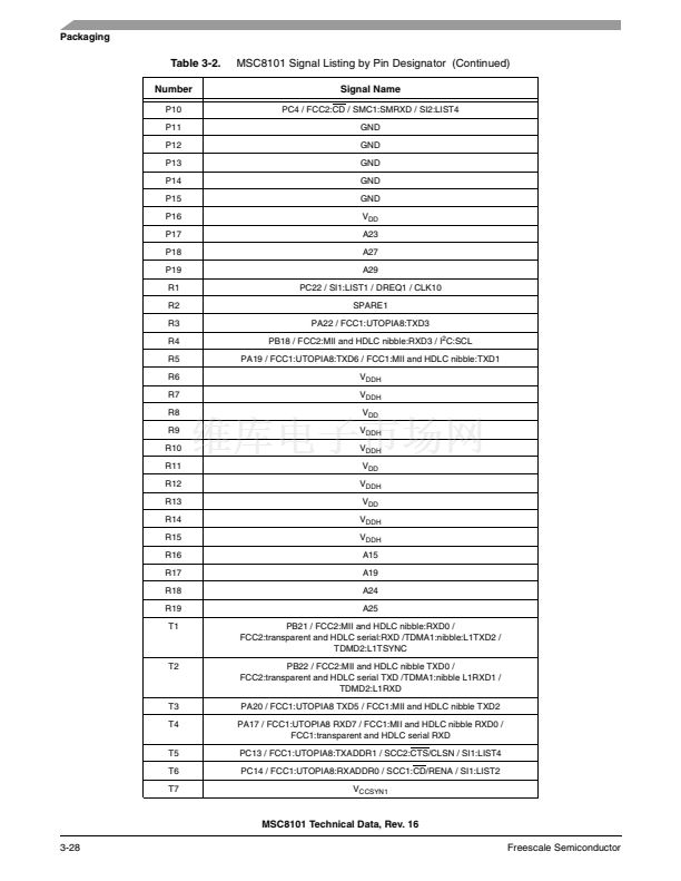
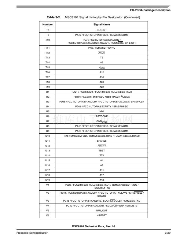
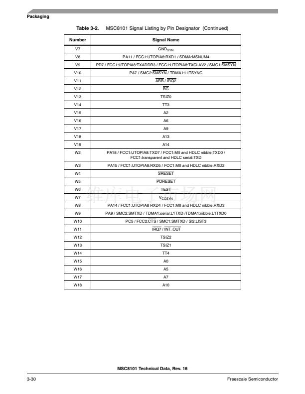
 1
1
 2
2
 3
3
 4
4
 5
5
 6
6
 7
7
 8
8
 9
9
 10
10
 11
11
 12
12
 13
13
 14
14
 15
15
 16
16
 17
17
 18
18
 19
19
 20
20
 21
21
 22
22
 23
23
 24
24
 25
25
 26
26
 27
27
 28
28
 29
29
 30
30
 31
31
 32
32
 33
33
 34
34
 35
35
 36
36
 37
37
 38
38
 39
39
 40
40
 41
41
 42
42
 43
43
 44
44
 45
45
 46
46
 47
47
 48
48
 49
49
 50
50
 51
51
 52
52
 53
53
 54
54
 55
55
 56
56
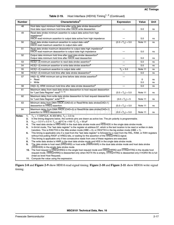 57
57
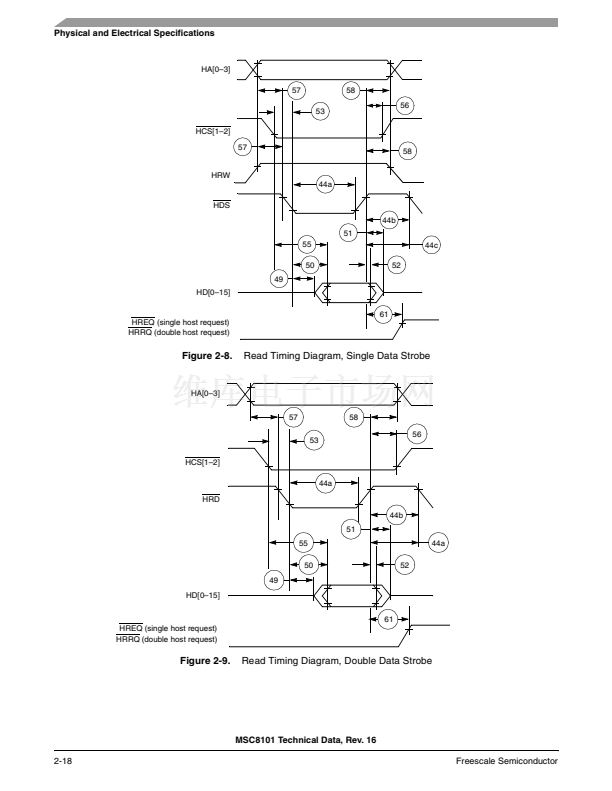 58
58
 59
59
 60
60
 61
61
 62
62
 63
63
 64
64
 65
65
 66
66
 67
67
 68
68
 69
69
 70
70
 71
71
 72
72
 73
73
 74
74
 75
75
 76
76
 77
77
 78
78
 79
79
 80
80
 81
81
 82
82
 83
83
 84
84
 85
85
 86
86
 87
87
 88
88
 89
89
 90
90
 91
91
 92
92
 93
93
 94
94
 95
95
 96
96
 97
97
 98
98
 99
99
 100
100
 101
101
 102
102
 103
103
 104
104
